Lab 2 - EE 421L
It was
required of us to download the lab2.zip file, unzip the files, and add them to
the directory in Cadence. While doing this I added the statement "DEFINE
lab2 $HOME/CMOSedu/lab2" to the cds.lib using notepad. I opened up
cadence, followed by opening up the sim_ideal_ADC_DAC which was uploaded when I
added the lab 2 file in the directory.
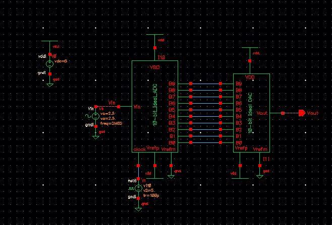
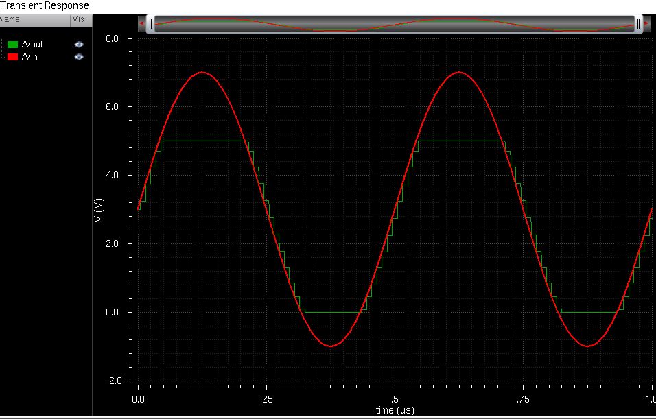
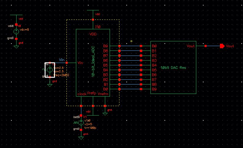
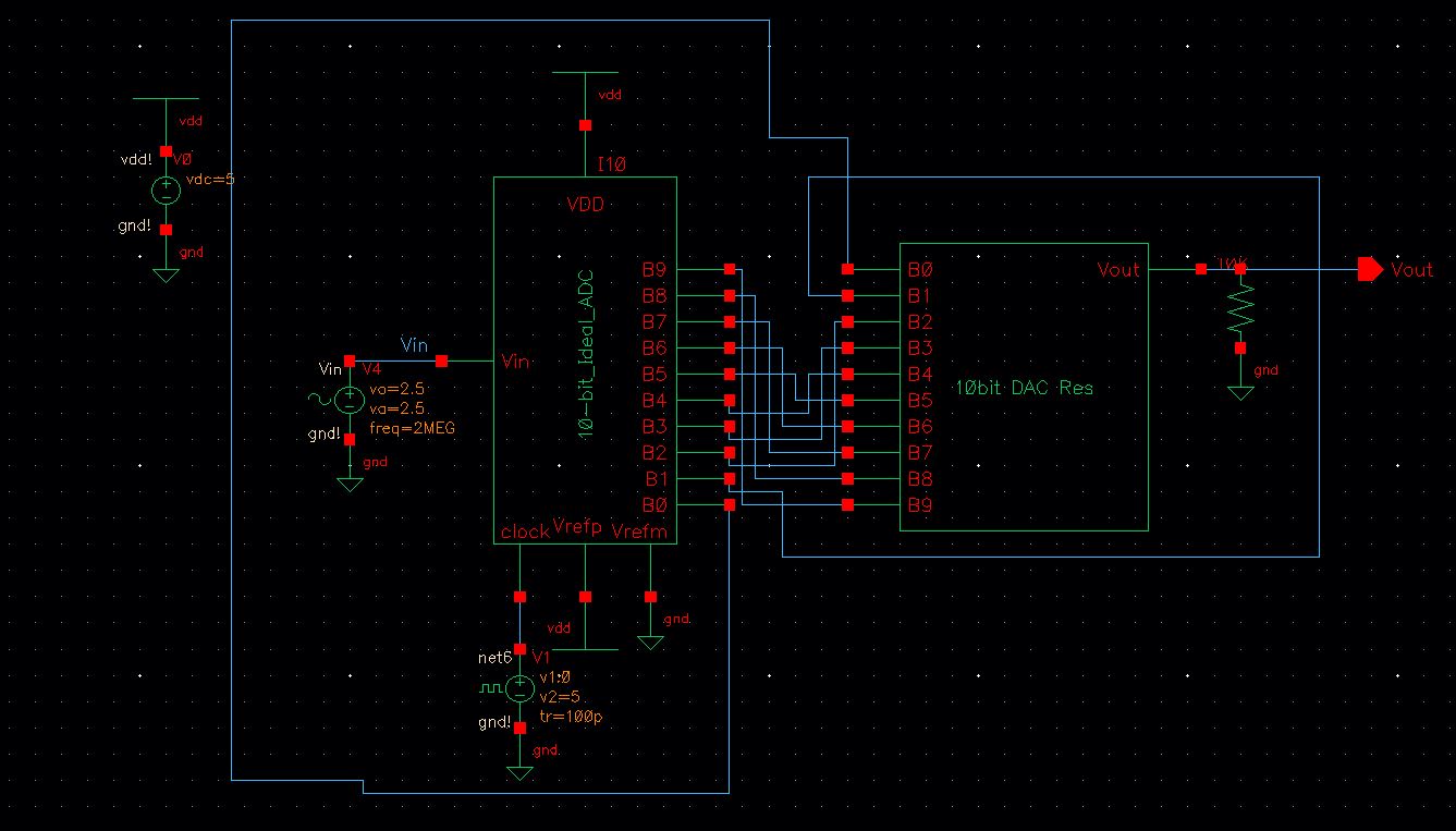
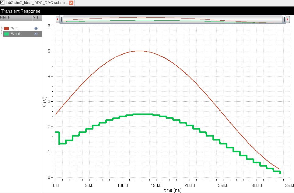
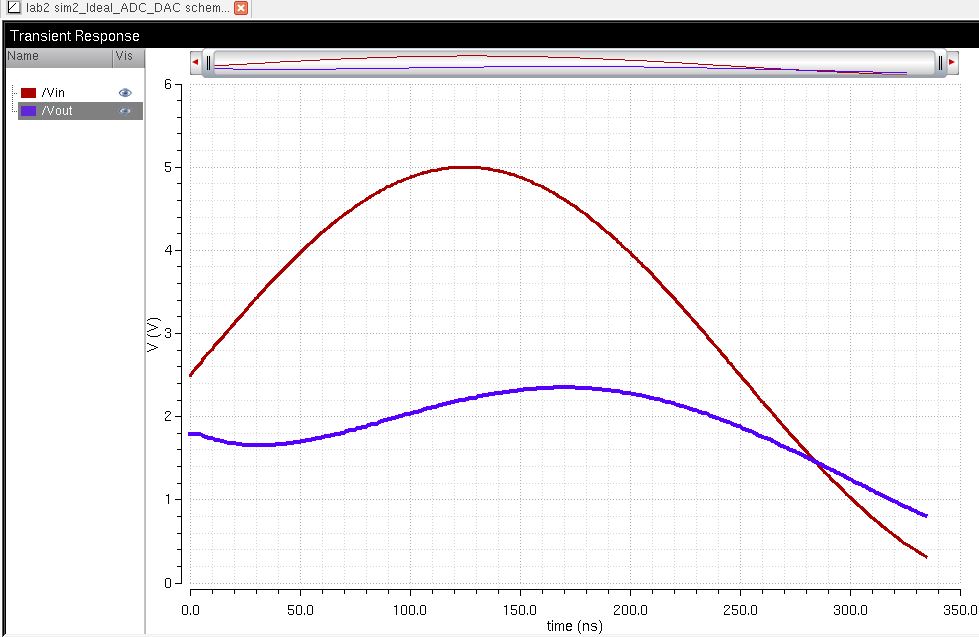
In the graph we have a Vin being inputted to the 10-bit ADC.
The output is taken as an input to the 10-bit DAC. Basically what is occurring
is there is an analog signal that is being converted to a digital signal, then
back to an analog signal.
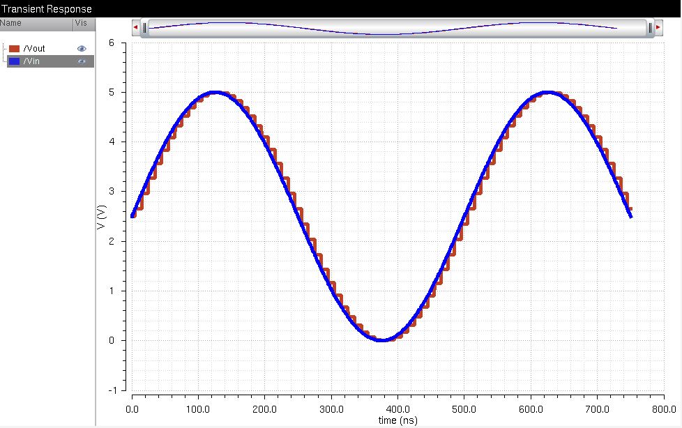
I also experimented with the graph and trace properties
which allows you to change the colors of the graph and lines, shape,
and thickness of the lines themselves too.
| |
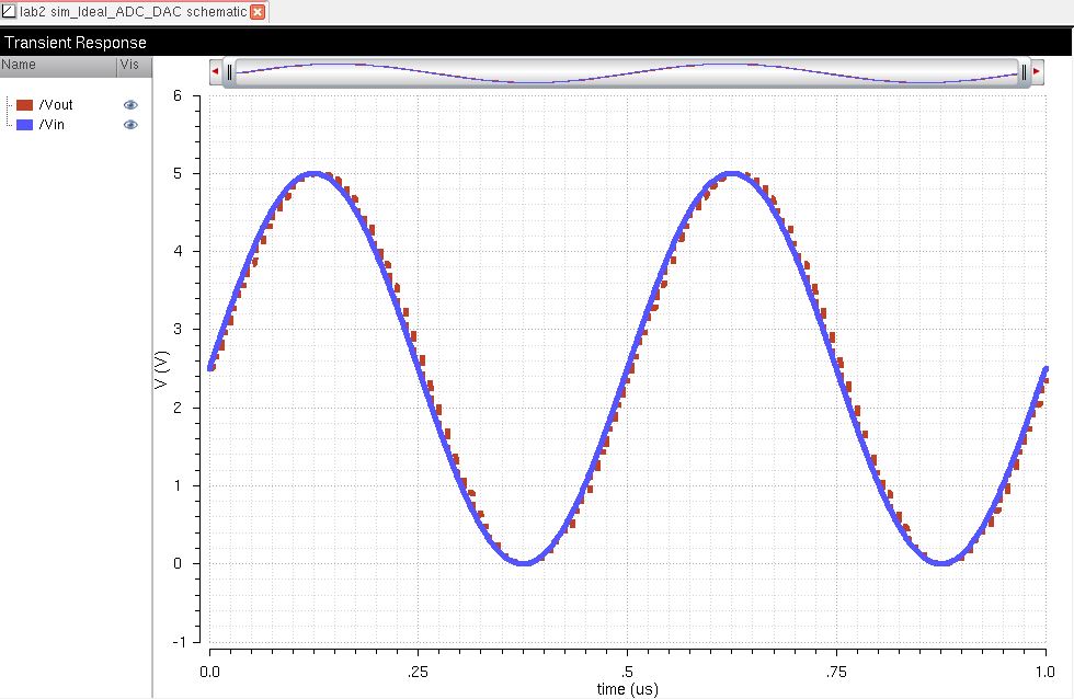
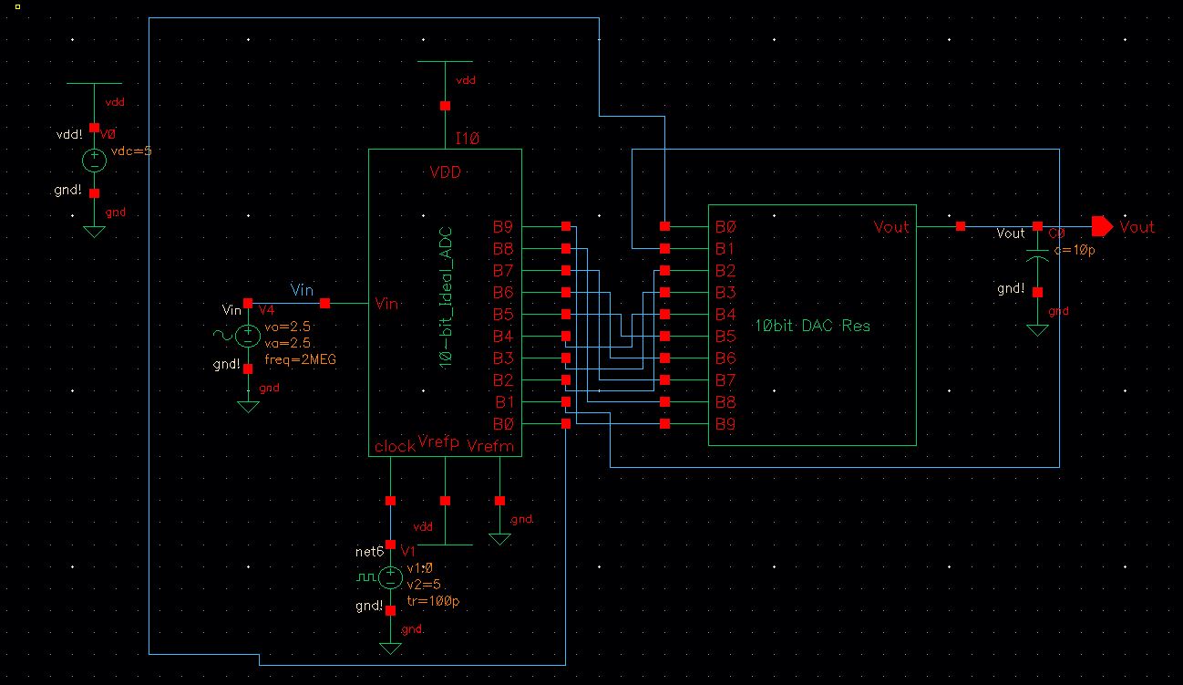
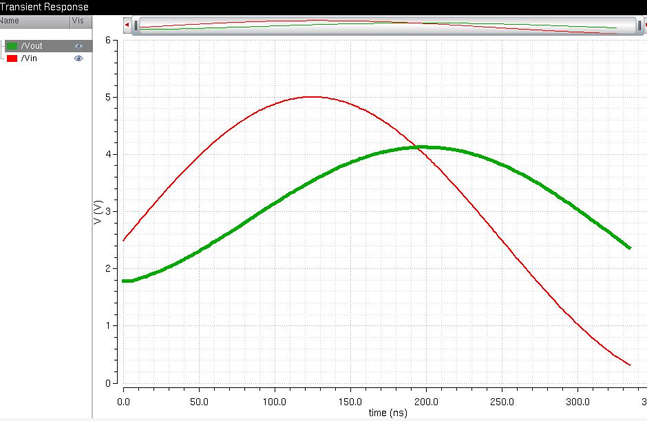
In the image below I modified Vin to have an offset of 3V and an
amplitude of 4V. It is meant to show how Vout cannot be higher than 5V because
Vdd is still at 5V. This causes clipping since the offset and amplitude that
was changed will cause Vout to exceed 5V.
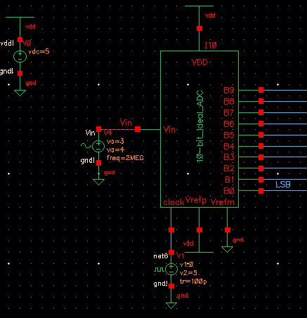
The least significant bit is the least voltage change on
the ADC or DAC to convert to a bit.
To determine the LSB we use the equation (Vdd/2^N).
Since we are using 10 bit devices the equation is (5/2^10) = 4.9mV
  |
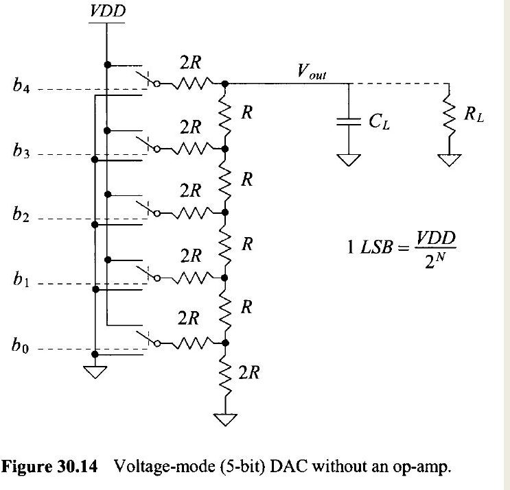
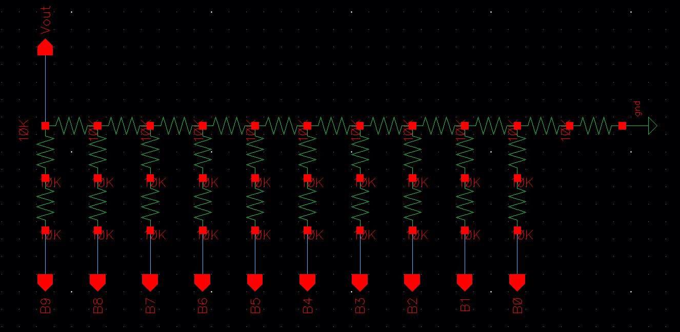
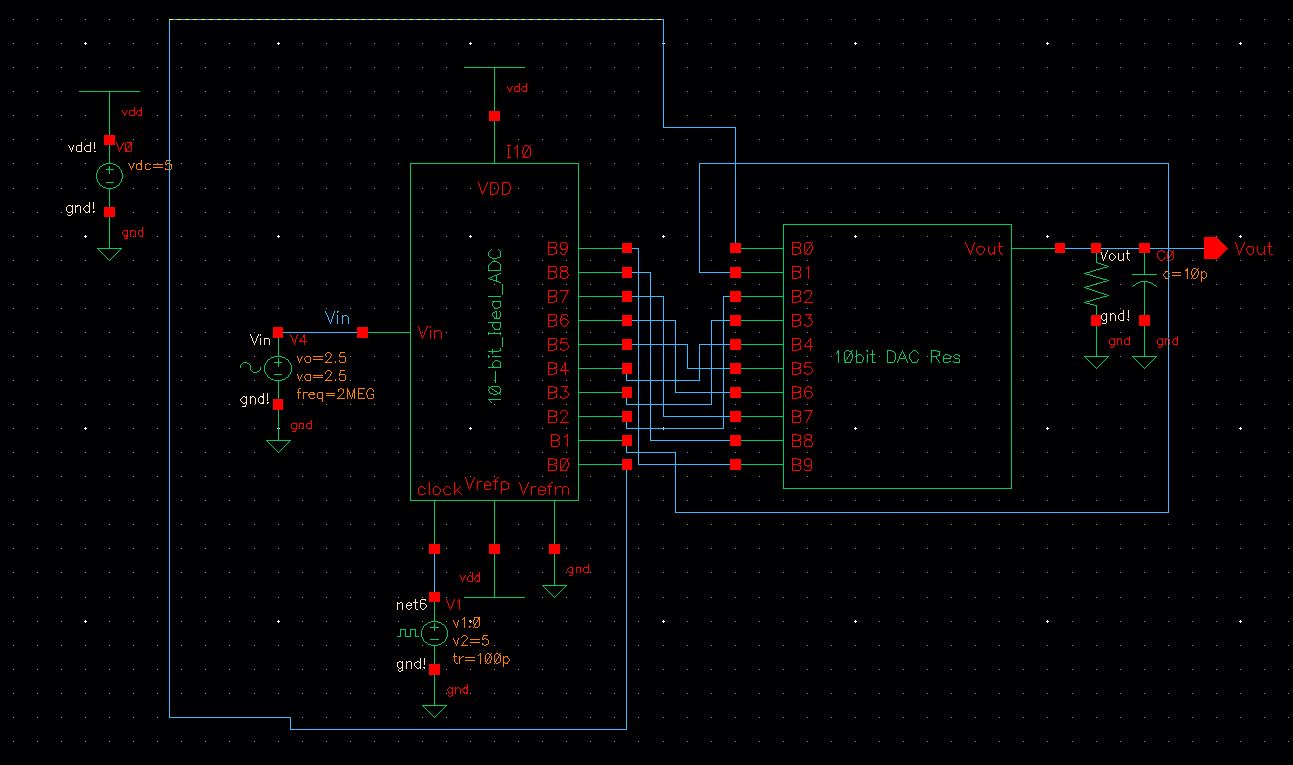
To start the lab off we were required to design our own
10-bit DAC using an n-well R of 10k. I followed the diagram shown below to
create my own but making a 10 bit DAC instead of the 5-bit one shown. I put two
10k resistors in series to create the 2R shown and when I finished I checked
and saved it.
To determine the output resistance I did the calculations starting on the far
right side combining the resistors in parallel and in series. We start by doing
the 2R||2R = ((2R*2R)/(2R+2R)) = 1R. Then we put it in series with the next R
and we have 2R again. We put this in parallel with the next section and keep
this repeating 10 times to get the output resistance of 1R.
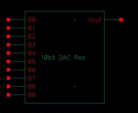
I then made a symbol out of the 10-bit DAC I just created.
This was done by going to create > cellview > from cellview > and then
hitting ok. I labeled it "10 Bit Res".
  |
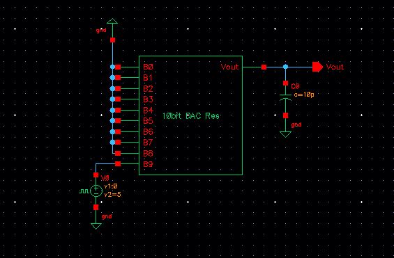
With my new
symbol created I then grounded all the DAC inputs except B9 which was connected
to a pulse source (0V-5V). To acquire the delay, that the DAC has driving
a 10 pF load, I used 0.7RC to get a rough estimate.
0.7RC = 0.7(10k)(10pF) = 70n
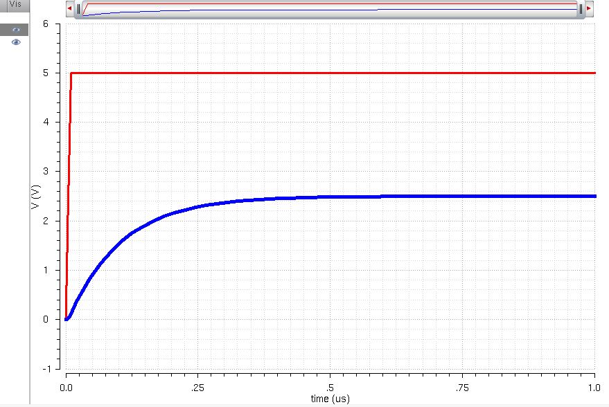
If we look below at 70ns, the output voltage is about 1.25V.
 |  |
Now to determine if my designs are functioning correctly I
started by copying the schematic cell
view sim_Ideal_ADC_DAC to a cell sim2_Ideal_ADC_DAC
and replacing the ideal DAC with the one I designed. The results were spot on,
the simulation looked just like the original sim_ideal_ADC_DAC's.
 |  |
I then added a resistor of 10k to where Vout is and
simulated it again. Adding a 10k load actually adds another voltage divider
which mean the Vout will be cut in half.
 |  |
 |  |
 |  |
If the resistance of the switches isn’t small compared to R, current will decrease and resistance will increase when the switches are closed. This will ultimately leave Vout to decrease as well.
My files will also be backed up in my student drive.