Project: 9-bit Even Parity Checker - ECE 421L
Authored
by Dominic Hryciuk,
email: hryciuk@unlv.nevada.edu
Last edited on 15 November 2017
This report details the design and operation of an 9-bit even parity checker with 8-bit data and 1-bit parity.
Theory of Operation:
The
purpose of a parity checker is to detect errors in transmission. The
parity checker circuit will determine whether the total number of
logical "1"s is even or odd at the end of transmission. This number is
then compared to a parity bit, which was created by a parity generator
and indicates the number of bits before transmission. If the numbers
match, no errors occured; if the numbers differ, an error has occured
somewhere in the data.
The design will be designed to output a "1" if the parity matches, and a "0" if not.
XOR gate design:
A
parity checker is designed by using XOR gates on the bits of the data.
An XOR gate will output a "0" if bits are similar, or a "1" if the bits
differ. This can also be interpreted as checking if two bits contain an
even or odd amount of "1"s.
XOR operation can be described in the table:
| A | B | X | Even? |
| 0 | 0 | 0 | Yes |
| 0 | 1 | 1 | No |
| 1 | 0 | 1 | No |
| 1 | 1 | 0 | Yes |
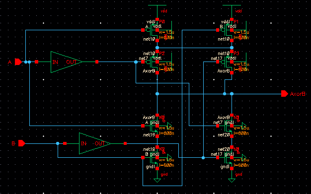
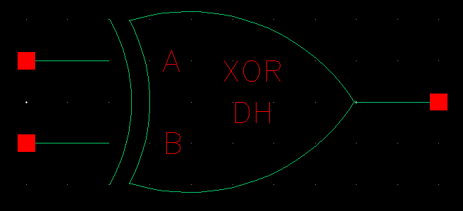
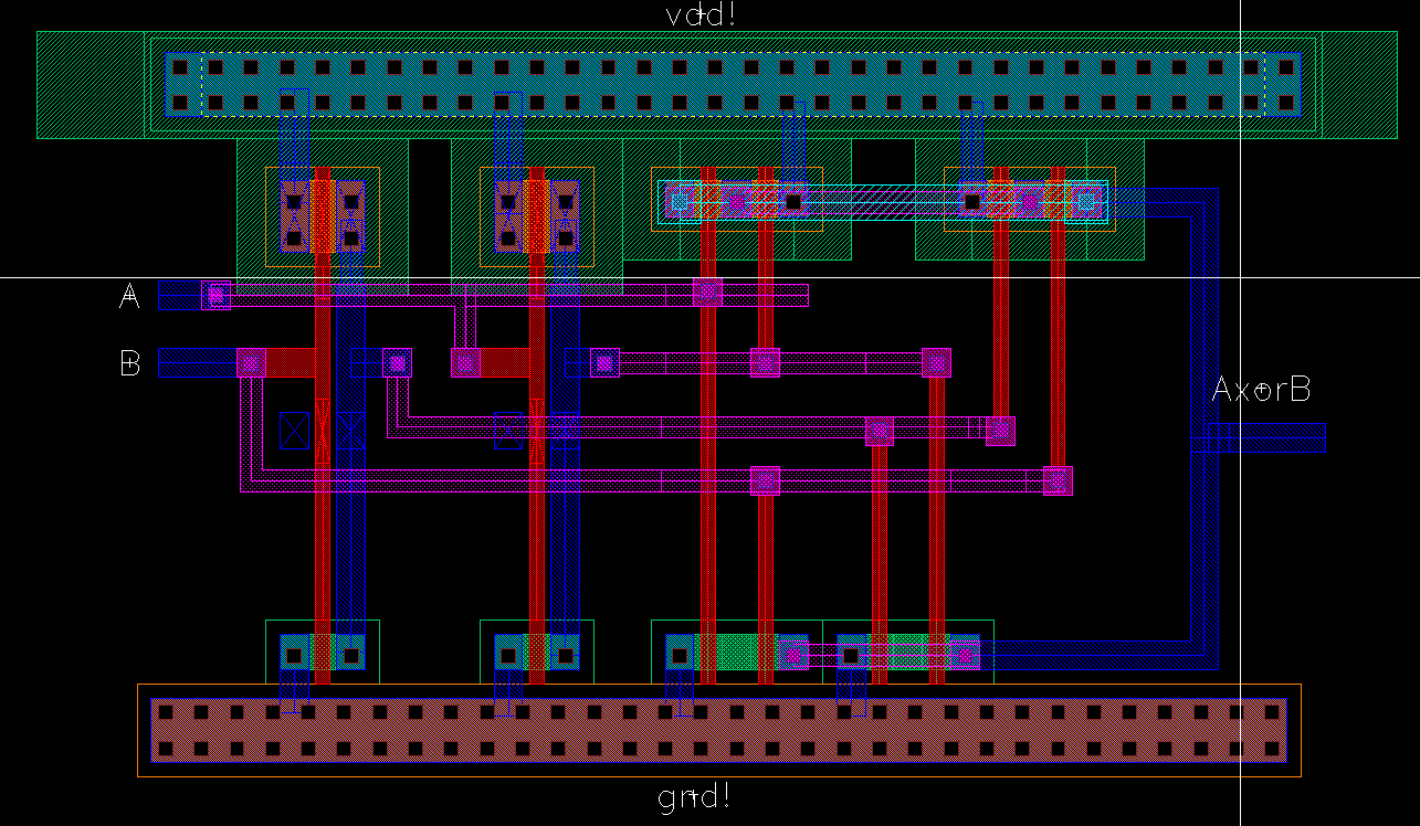
The XOR gate is created using PMOS and NMOS compliments, and created into a symbol for instantiation:
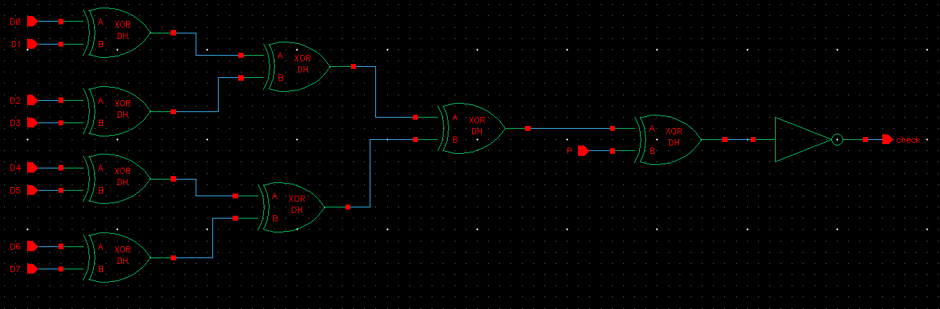
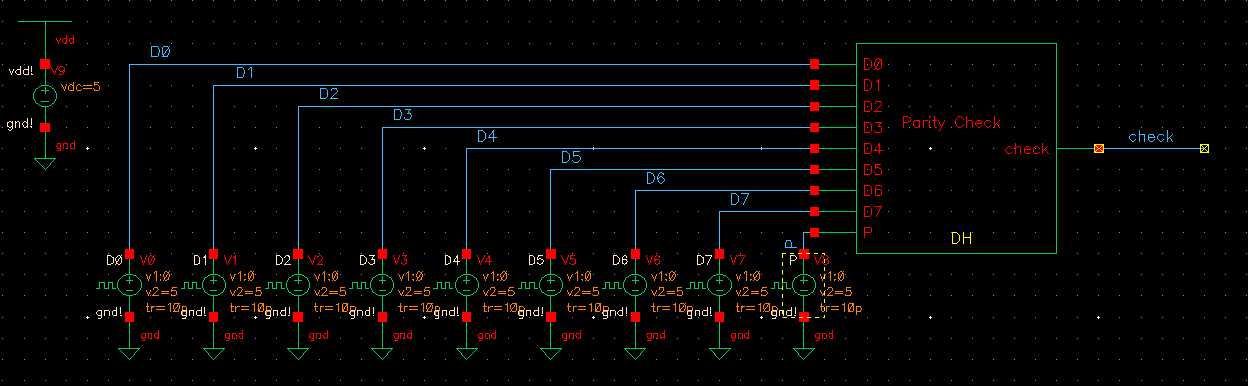
Parity Checker Design:
The
input word of the parity checker is 8-bits of data and 1-bit parity.
The data is XOR'd with itself to check if the data is even and then
XOR'd with the parity bit. The schematic of the circuit is shown below:
The
circuit outputs a "1" if the number of bits (even or odd) matches the
parity bit received, and thus no errors occured. It will output a "0"
otherwise, indicating an error in transmission. The operation of the
cicuit is condensed into the table below:
| Data | Parity | | Check? |
| Even | 0 | | 1 |
| Even | 1 | | 0 |
| Odd | 0 | | 0 |
| Odd | 1 | | 1 |
This
operation is the XOR logic table inverted. Design constraints require
the output to be "1" when the parity matches and "0" when they don't.
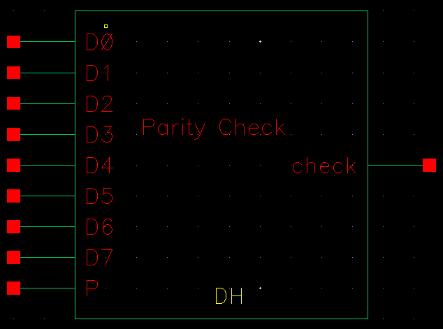
A symbol of the parity checker is created for simulation:
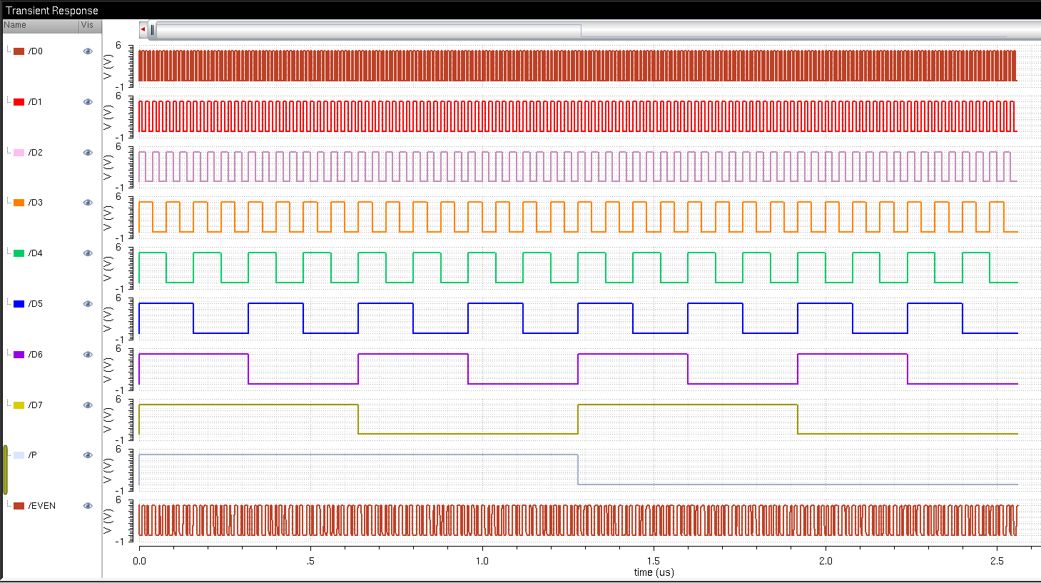
Simulation:
The circuit is simulated by allowing the data bits to vary through all
possible combinations. This allows a simulation to view all 256
possible bit combinations at once, with odd and even parity bit.
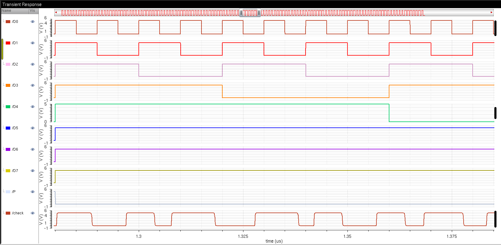
The
simulation can be zoomed in to view more detailed operation. The zoom
in is done where the parity bit is 0, i.e. for even parity check:
The
circuit is operating correctly. However, the output has a noticable
delay. This is due to the logic circuitry and the inverter used in the
parity check. This can be measured by looking at the time from a bit edge to when the output changes:
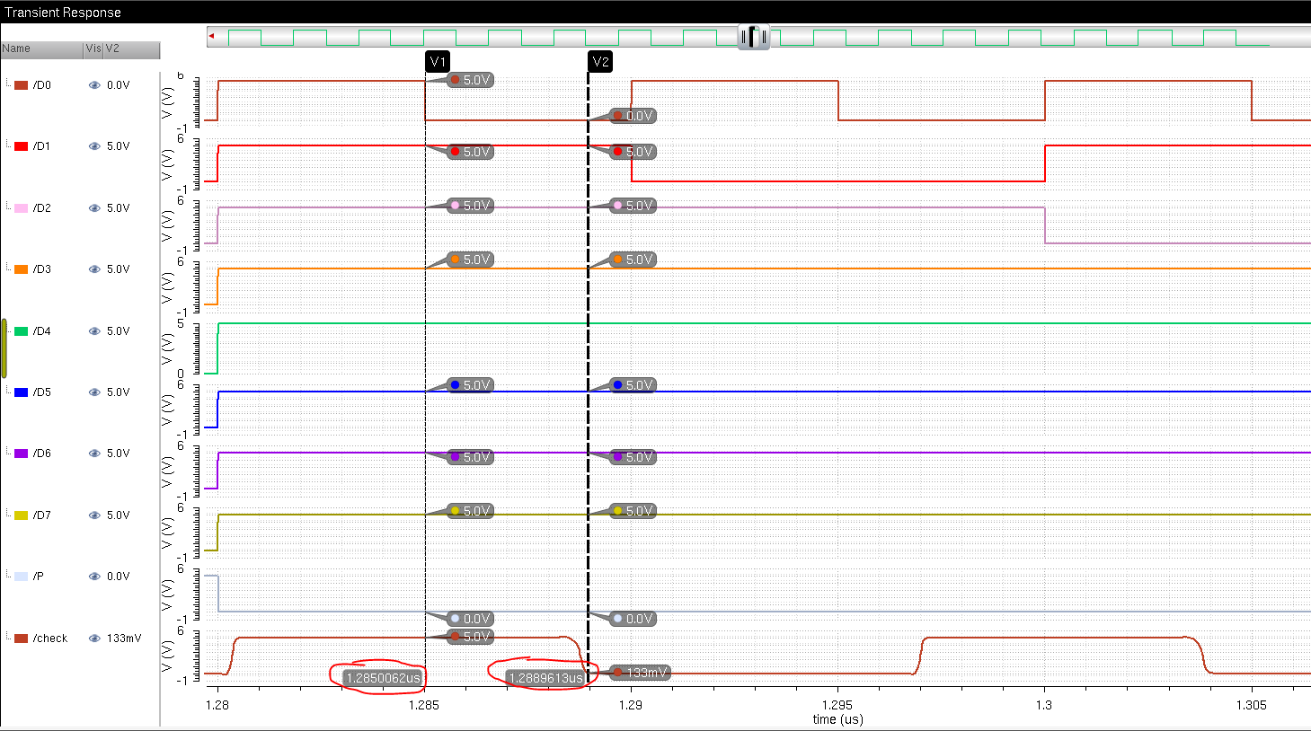
The delay is measured to be about 3 ns from propagation of the signal by using markers on the simulation.
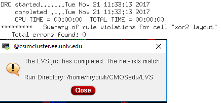
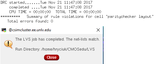
Layout:
The
layout for the parity checker instantiates the XOR cell shown below and
interconnects it to create the parity checker circuit. It passes DRC
and LVS checks.
The parity checker instantiates 8 XORs and an inverter, which can be laid out in a 2x4 array, with inputs D0-7 on the left and check on the right. It passes DRC and LVS checks.
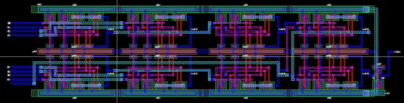
The
layout is connected to a padframe, with inputs and outputs connected to
pins for fabrication. The connections to pins are documented below:
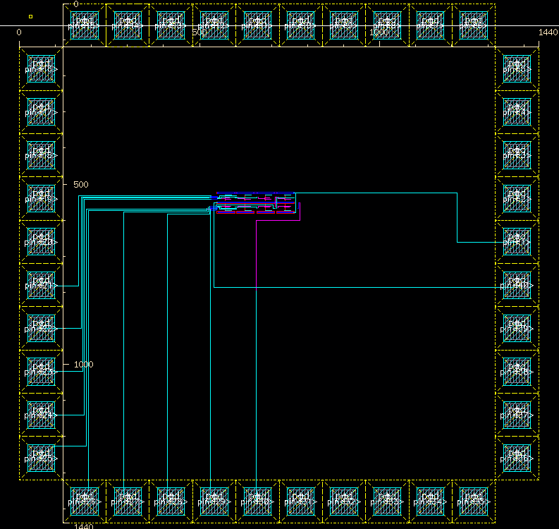
| Pin Number | Pin Name |
| pin<1> | vdd |
| pin<21-28> | D<0-7> |
| pin<29> | P |
| pin<30> | check |
| pin<40> | gnd |
The design files used in this project can be found at the link: Hryciuk_proj.zip
Return to EE 421L Labs
Return to Student Directory