Lab 6: Design of CMOS NAND, XOR and Full Adder - ECE 421L
Authored
by Dominic Hryciuk,
email: hryciuk@unlv.nevada.edu
Last Edited on 25 October 2017
The
purpose of this lab is to draft the schematics and layouts of a 2-input
NAND gate and 2-input XOR gate, test their operation, and instantiate
the designs to create a full adder.
The
logic gates are created using MOSFETs of 6u/0.6u size for both PMOS and
NMOS. Because the sizes are created the same, the logic circuitry will
carry logic lows quicker than logic highs. This is because of the
higher inherit resistance per unit square of a PMOS; a PMOS will have a
higher resistance than a PMOS if width and length parameters are the
same. A higher resistance means it will have a lower flow of current.
This difference will be apparent in simulations of the devices.
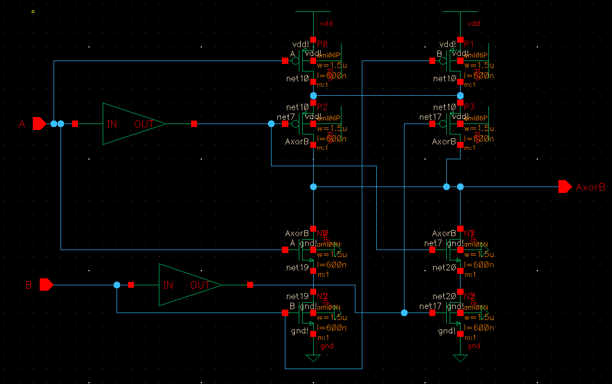
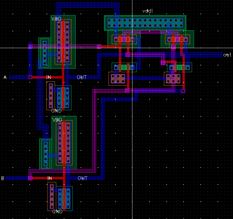
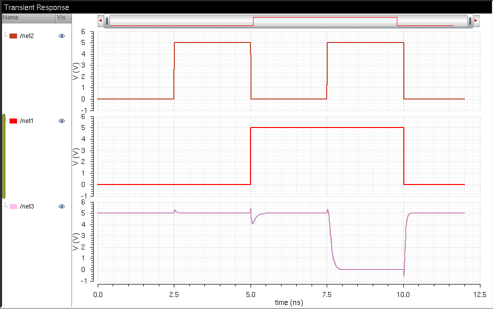
The
2-input XOR gate is laid out using CMOS. PMOS is designed for the
condition where the gate should transmit a high; NMOS is designed for
the condition where the gate should transmit a low. The schematic,
simulation, layout and truth table are shown. Note that when the gate
switches from a low to a higher, it takes about twice as long to reach
steady state compared to switching from high to low:

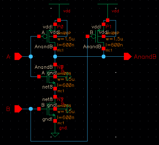
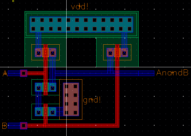
The 2-input NAND gate is laid out using CMOS.
The schematic, simulation, layout and truth table are shown. Like the
XOR gate, it takes about twice as long to transition from low to
high.
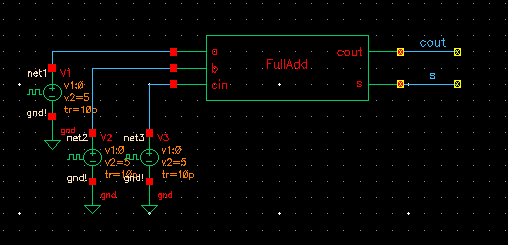
Symbol view are created from the XOR and NAND designs and instantiated to create a full adder.
The full adder schematic, simulation and truth table are shown below. A
longer simulation time was done to ensure that propagation and
switching was not an issue in operation.

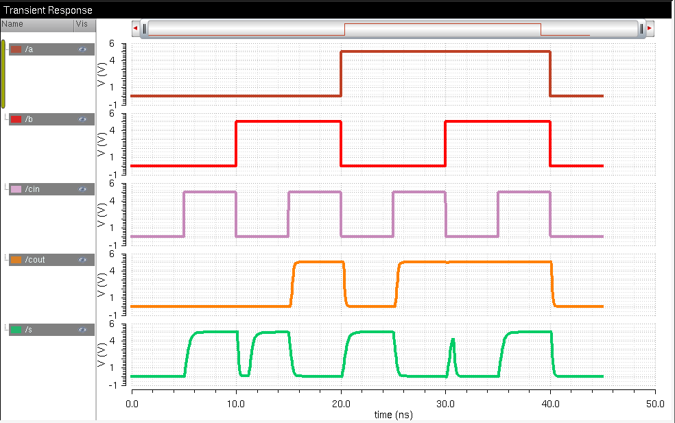
| A | B | Cin | sum | Cout |
| 0 | 0 | 0 | 0 | 0 |
| 0 | 0 | 1 | 1 | 0 |
| 0 | 1 | 0 | 1 | 0 |
| 0 | 1 | 1 | 0 | 1 |
| 1 | 0 | 0 | 1 | 0 |
| 1 | 0 | 1 | 0 | 1 |
| 1 | 1 | 0 | 0 | 1 |
| 1 | 1 | 1 | 1 | 1 |
The design files can be found in the lab6.zip.
Return to EE 421L Labs
Return to Student Directory


