Lab 5 - ECE 421L 

Authored by Dominic Hryciuk,

email: hryciuk@unlv.nevada.edu

Last edited by 11 October 2017


The purpose of this lab is to design, layout and simulate different CMOS inverters.


CMOS inverters have two complementary sides to a layout: PMOS connected to VDD, and NMOS to ground. This is deliberately done as PMOS devices transmit highs better, and NMOS devices transmit lows better.

The signal which is being inverted controls the gates of both the MOS devices. An active signal will cause the NMOS to pull the output to ground, while a low/no signal will cause the PMOS to pull the output to VDD.


Inverters of two different sizes will be drafted: 12u/6u, and 48u/24u. The PMOS device is larger than the NMOS device to keep resistances equivalent; the channel of PMOS has approximately half the resistance of NMOS.


Schematics for both inverters are created, with a multiplied used for the larger inverter. Symbols are also created:


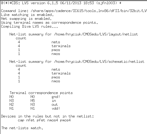
The difference between the two inverters is more noticable in layout, where the 48u/24u inverter is larger. The layouts pass LVS testing:


Simulations of the inverter driving a capacitive load are performed. The capacitor has values of 100fF, 1pF, 10pF, and 100pF.

Simulations are performed started with the smallest capacitive value and increasing.

For the 12u/6u inverter:


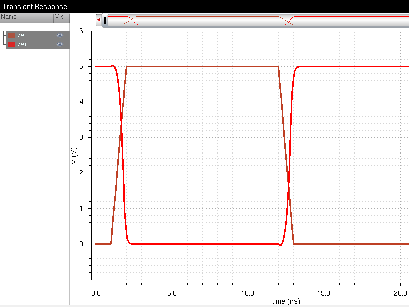
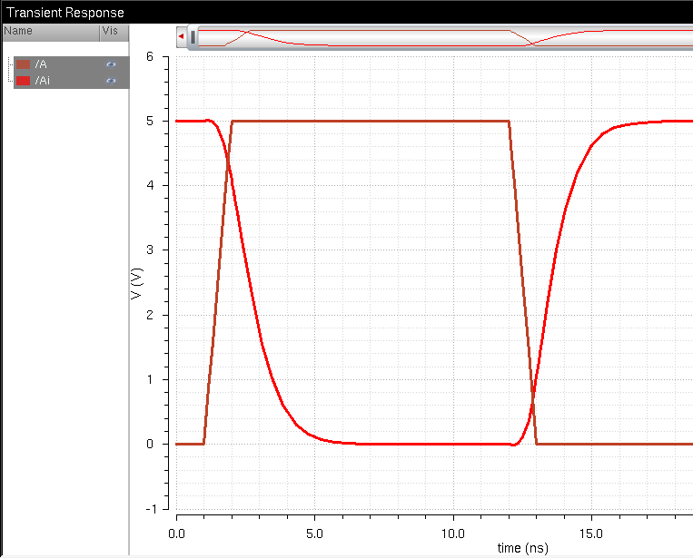
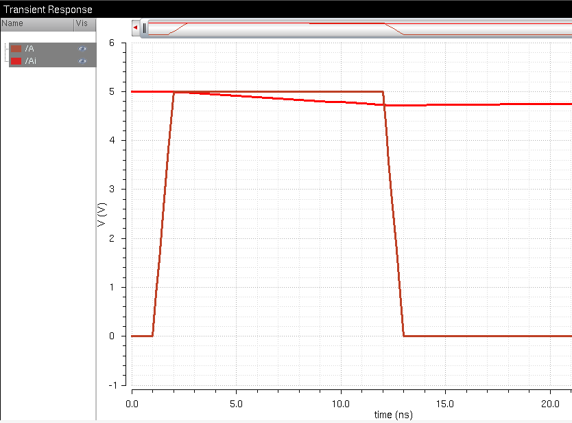
As the capacitor value increases, the inverter takes longer to reach steady state values. At 10pF and beyond, the inverter doesn't respond fast enough before the pulse changes.

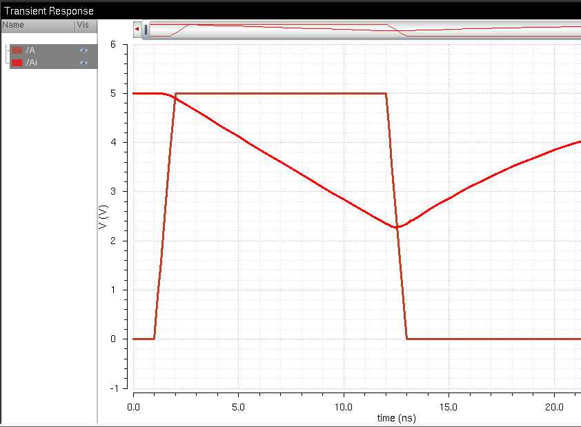
For the 48u/24u inverter:


Compared to the other inverter, the larger 48u/24u can handle larger capacitive loads. It has wider NMOS/PMOS devices, and thus lower resistance. With a lower RC time constant when switching, the system can respond fast enough for larger capacitive loads. The inverter still cannot respond fast enough for a 100pF load.


The design files used for this lab can be found in lab5_dh.zip


Return to EE 421L Labs


Return to Student Directory