Lab 2 - ECE 421L
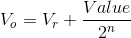
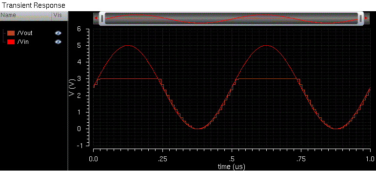
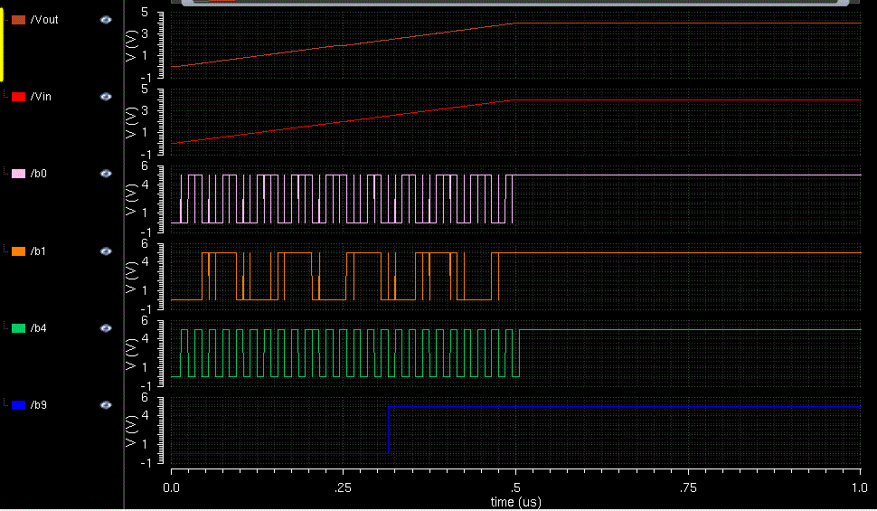
When simulated, Vout makes in steps rather than continuously changing. The output is dependent on both the input and the reference voltage in the following relationship:
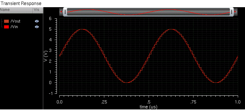
When the reference voltage changes, the output will only operate up to the reference voltage. When VDD is dropped to 3V, the waveform is capped.
You can look at what order the bits in the DAC output change to tell which one is the least significant bit. The first one to change is the least significant; the last one to change is the most significant bit.
The equation for the least significant bits is:

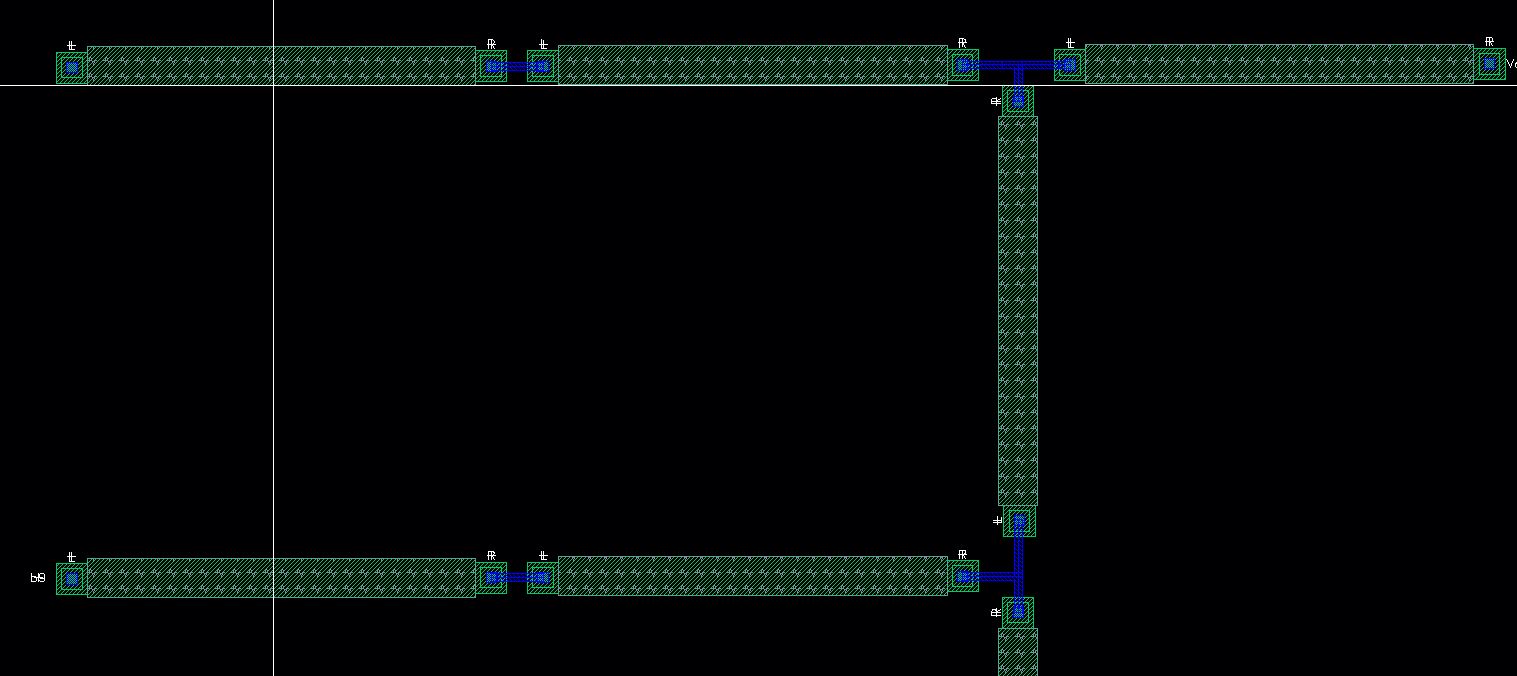
The 10-bit DAC is redesigned using the R-2R layout with 10k n-well resistors. The most significant bit is at the top. The actual layout emulates the schematic, so it is not as compact as it could be.

click for a larger image
The output resistance of this schematic can be determined by setting all of the pins to ground, and combining resistors in parallel and series. When doing so, you'll be repeating the same two operations until you are left with one resistor, R.


The schematic can be represented as a small symbol, allowing it to be easily implemented into other designs.

When connected to a capacitive load, the DAC will have a delay when a pulsed source is placed on one of the bits. This delay is approximated by 0.7RC, where C = 10pf and R is the combined resistance of the R-2R ladder, which is 10k. The delay should be 70ns.
