Project - EE 421L
Authored :: Aaron Escobedo,
Email :: Escoba3@UNLV.Nevada.edu
Due :: November 15th, 2017
For
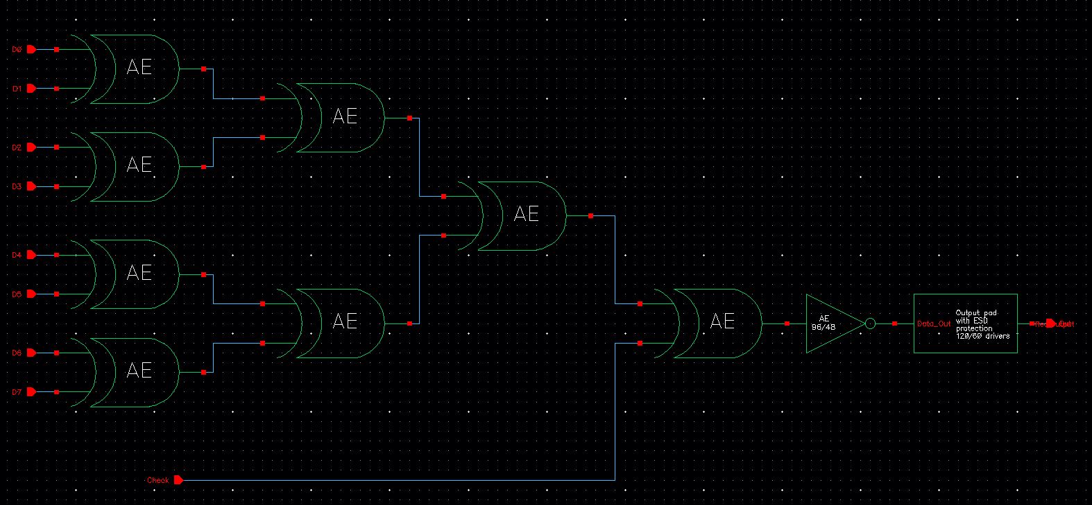
our project, we will be looking to implement a 9-bit parity checker -
in this, 1 bit is for checking while 8-bits are for data.
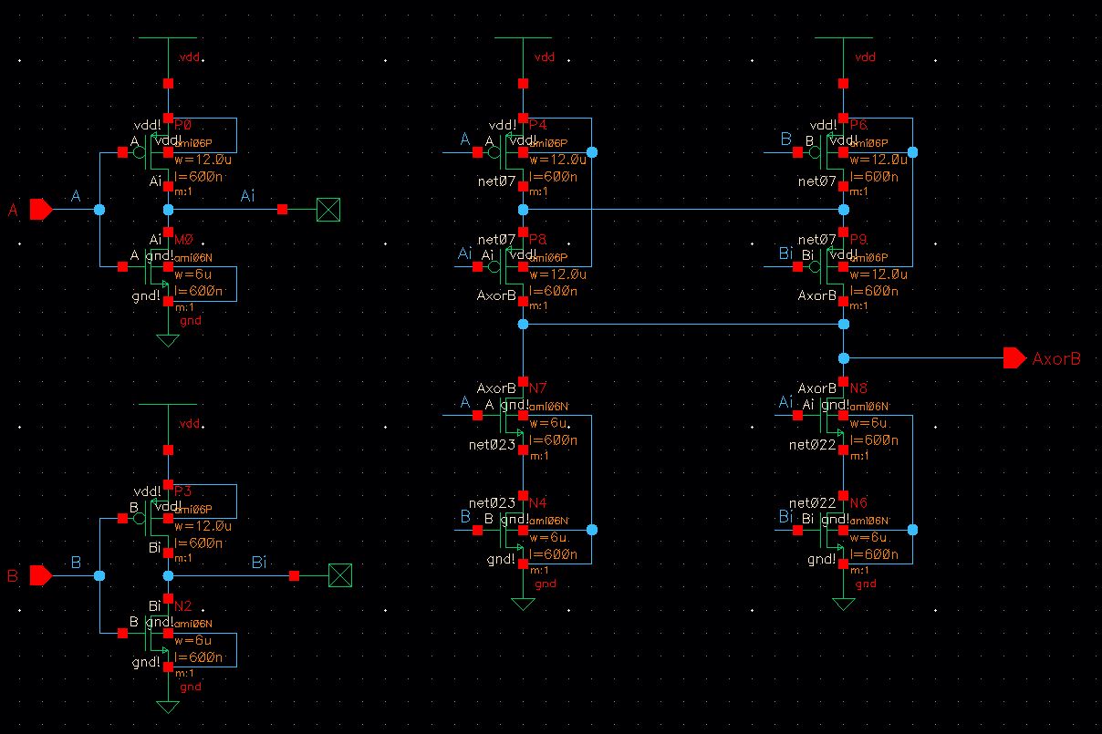
For
our implentation of a parity checker, we can use purely XOR logic gates
to create the logic we are looking for. one such implementation is now
shown below.
In
this schematic, I have reused many of the implemnted logic gates
previously created for other labs. the XOR gate is now shown below
which was previously used;
XOR Schematic | 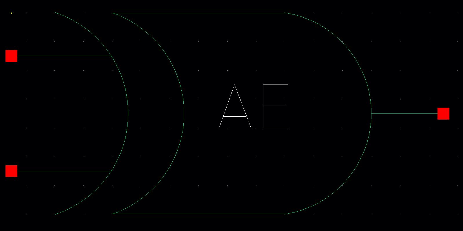
XOR Symbol | 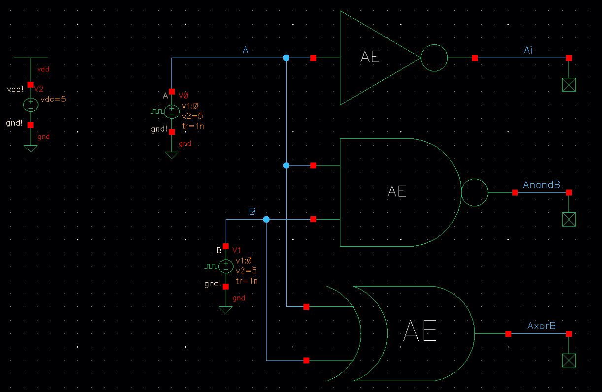
XOR Simulation Schematic | 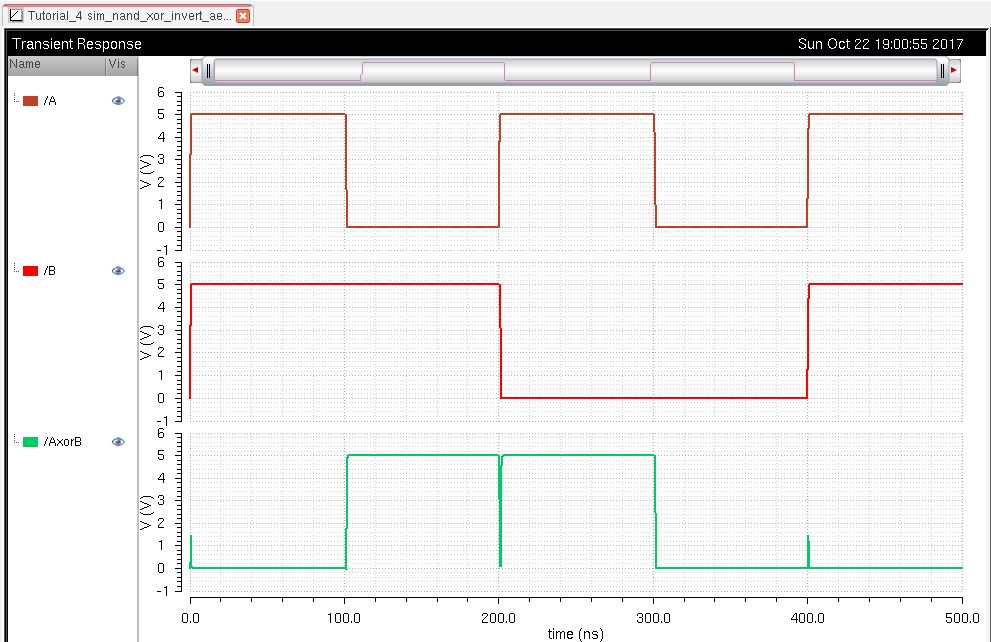
XOR Logic Results |
With
these results to showcase we have created an XOR logic gate, we were
able to implement them appropiately to be used for the parity checker.
Additionally,
we had to an inverter at the end of our circuit, however, a concern of
us is the output capacitiance for this circuit as at some point, the
user will desire to check the actual output of this circuit via a pad
with a oscilloscope probe. Since oscilloscope probes commonly have
approximately 10pF of capacitance, we would desire out output invert to
have close to 10pF of capacitance. We can achieve this via some
calulcations.
From the calculations, we can estimate a
value of 96/1 ratio for the PMOS device, while the NMOS device will use
a 48/1 ratio - this is represented as a 96/48 on the inverter symbol
itself.
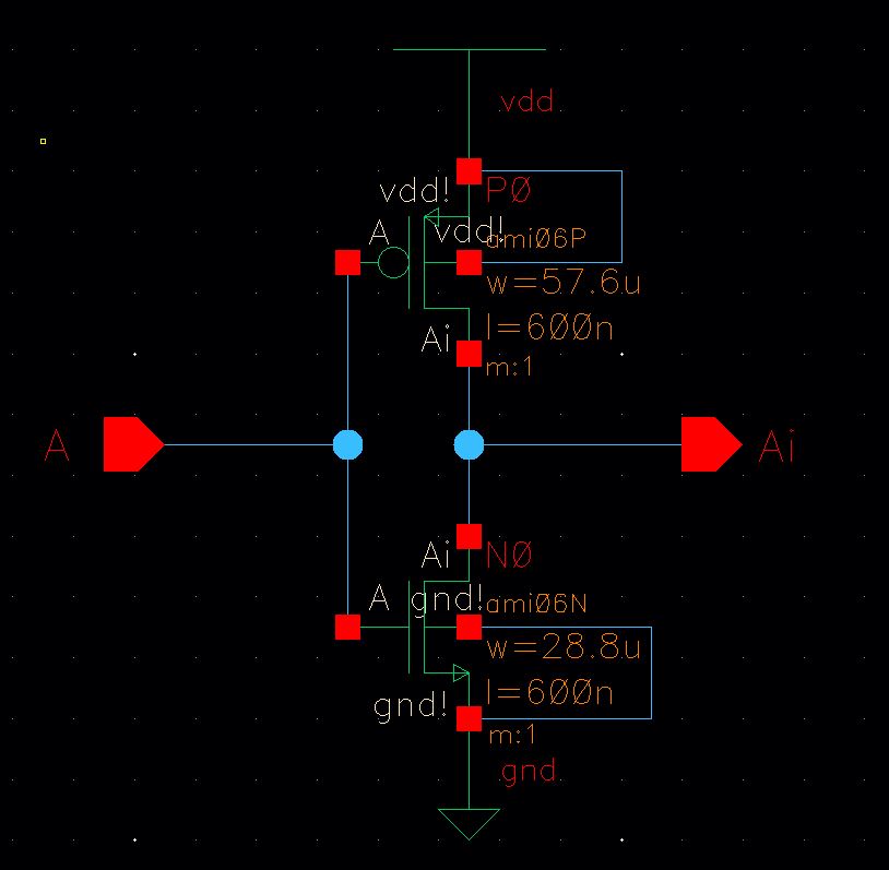
96/48 Inverter Schematic | 
96/48 Inverter Symbol |
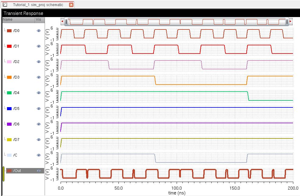
With all these in place, we can now create a symbol, and simulate our parity checker, the following now showcases my results;

Parity checker symbol | 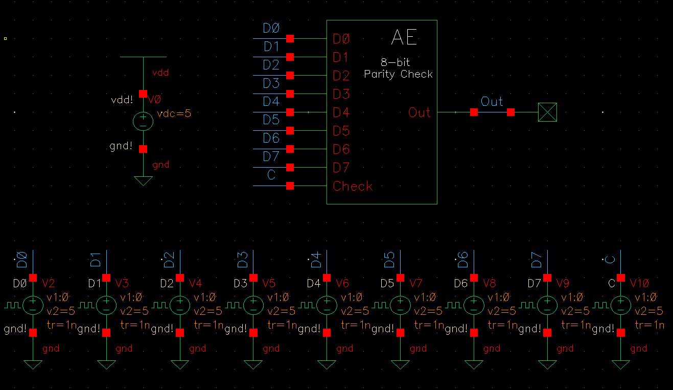
Simulation Schematic | 
Simulations Results - we can see various input options here |
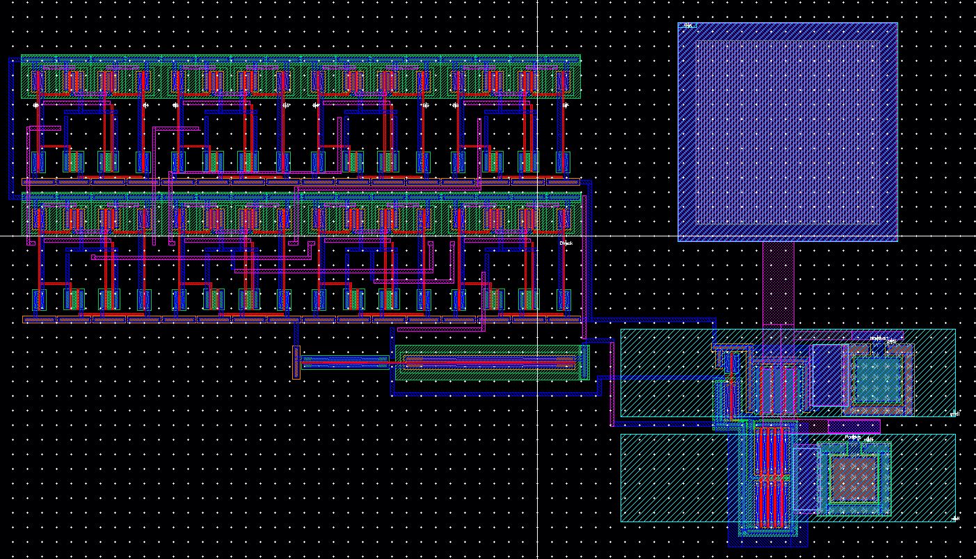
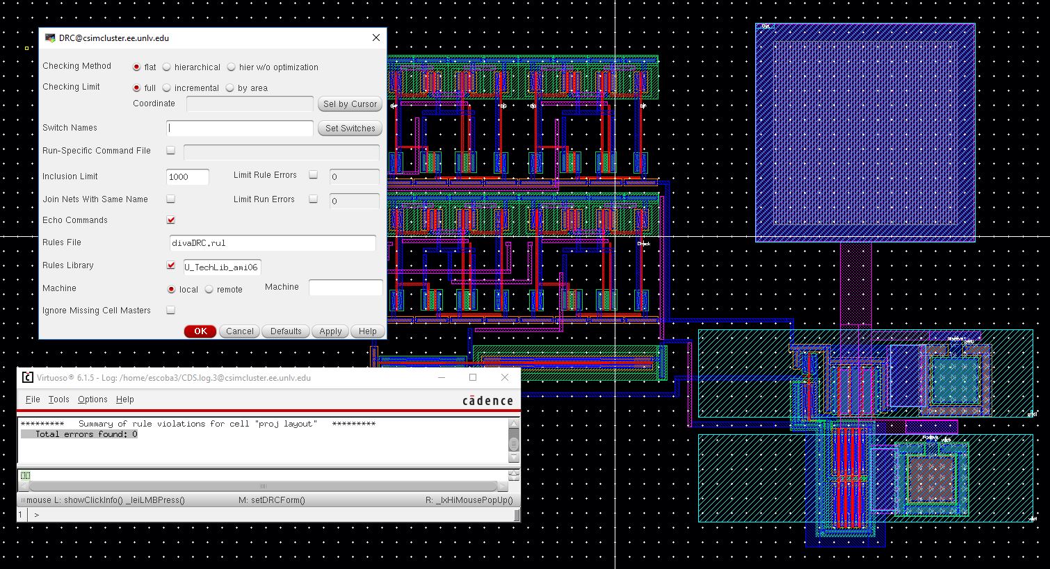
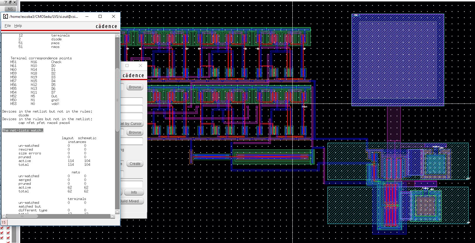
With this portion complete, I will now begin the process of implemented it from a layout perspective.
To start, I will once again use the XOR logic gate used previously; this layout and related extracted view is now is shown below
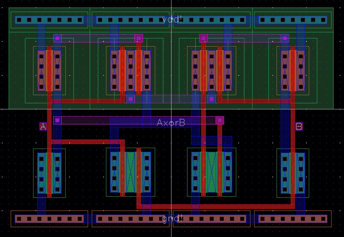
Layout of XOR | 
Extracted view of XOR |
In
addition to an XOR, we will need an inverter. Unlike previously though,
we will have a much larger inverter, so this had to be created from
scratch; this is now shown below
Since probes typically have a
internal capacitance of 10pF - we will want to match this 10pF load
with our circuit, our inverter then should be close to 10pF.
| General Delay Calculation | 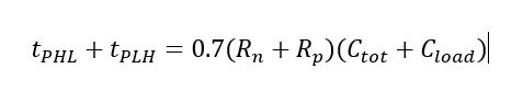 |
| Total Capacitance | 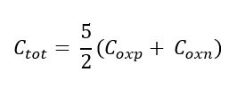 |
| Derivation of Coxn/p | 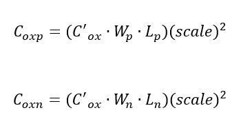 |
| Resistance for C5 Process | 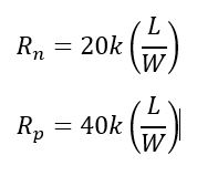 |
| Capacitance for C5 process | 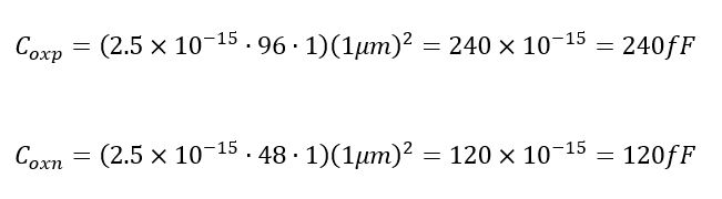 |
| Calcualted total capacitance | 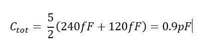 |
| Calculated resistance total | 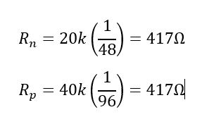 |
| Calculated total delay though inverter |  |
In
the above, we can see I used a 96/48 sized inverter - this was done to
get close to the expected value of the probe scope (10pF) as eventaully
we will have to measure our circuits implementation.
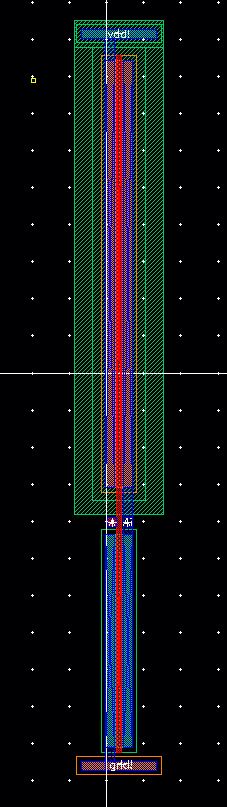
Layout of 96/48 Inverter | 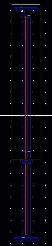
Extracted view of 98/46 Inverter | 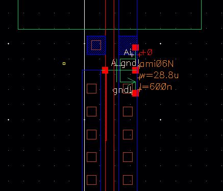
NMOS side of the 98/46 Inverter | 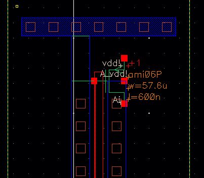
PMOS side of the 98/46 Inverter |
These values now match what we calculated previously and also used in our schematic
From
here, we can follow the schematic previously shown on the top of the
webpage to create a proper layout - however, we will also need to add
more. We need a way to physically measure the results of this layout
and as such, we will add an output pad with ESD protection.
Fortunately, this portion of the circuit was provided for us via the
CMOSedu website. The now updated schematic and corresponding layout
will look like this;
Return to Students
Return to EE 421L Labs