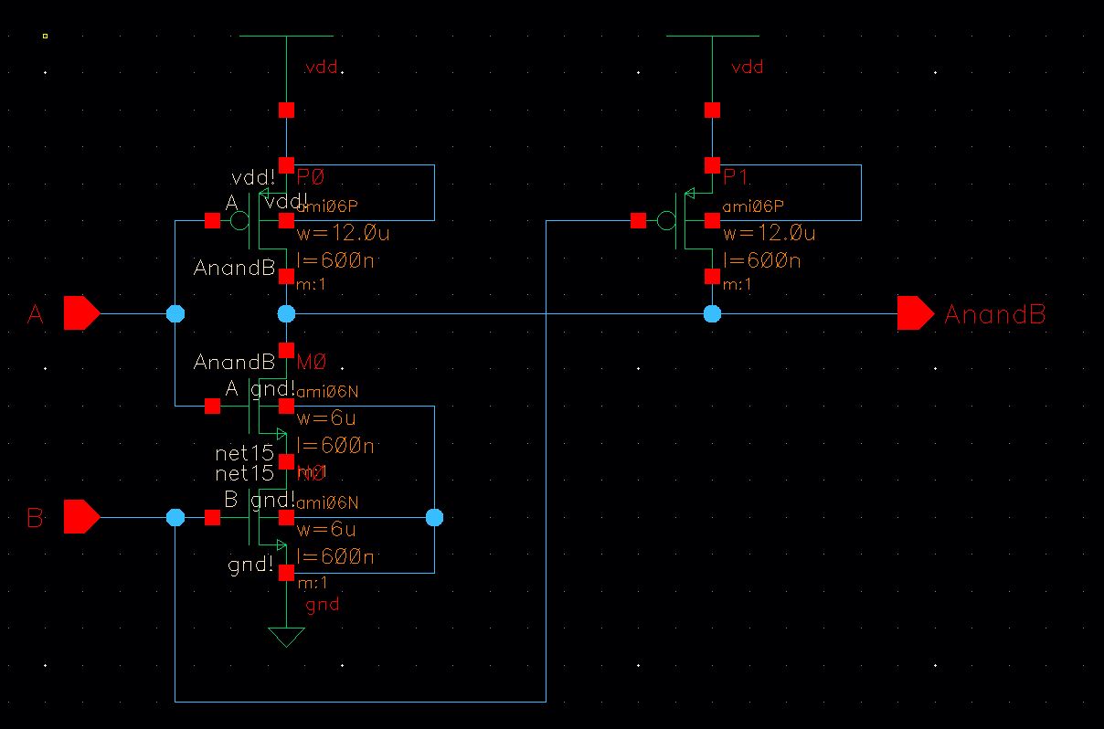
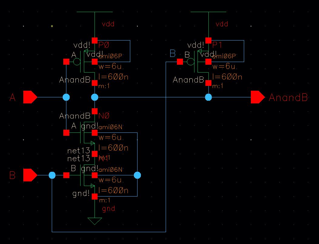
Nand Schematic View
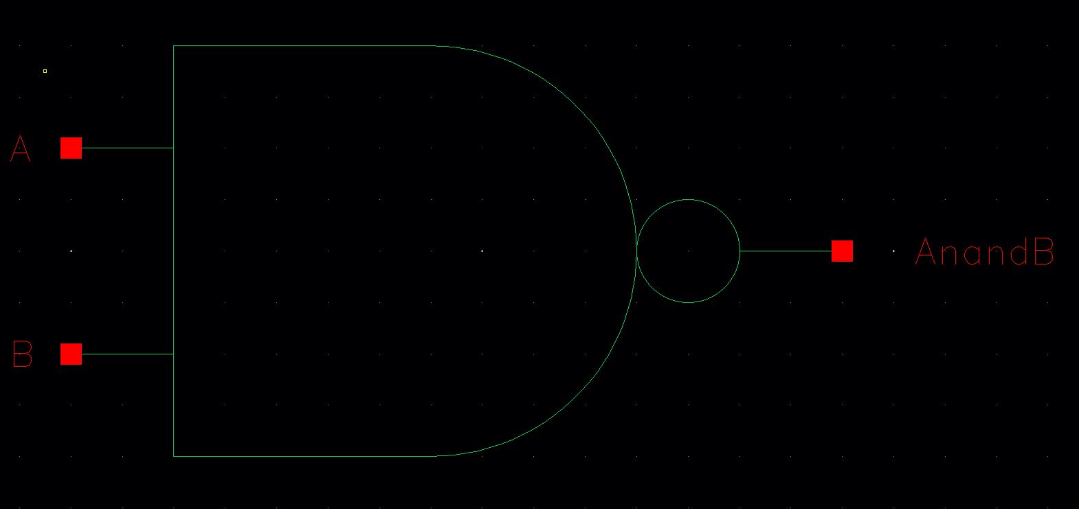
Nand Symbol View
Lab 06 - EE 421L
Nand Schematic View | Nand Symbol View |
 Nand Simulation Schematic |  Nand Simulation Results |
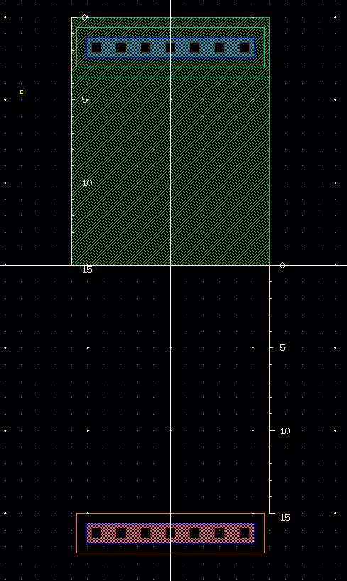
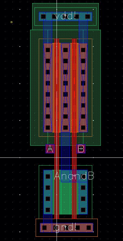 Layout view of Nand gate | 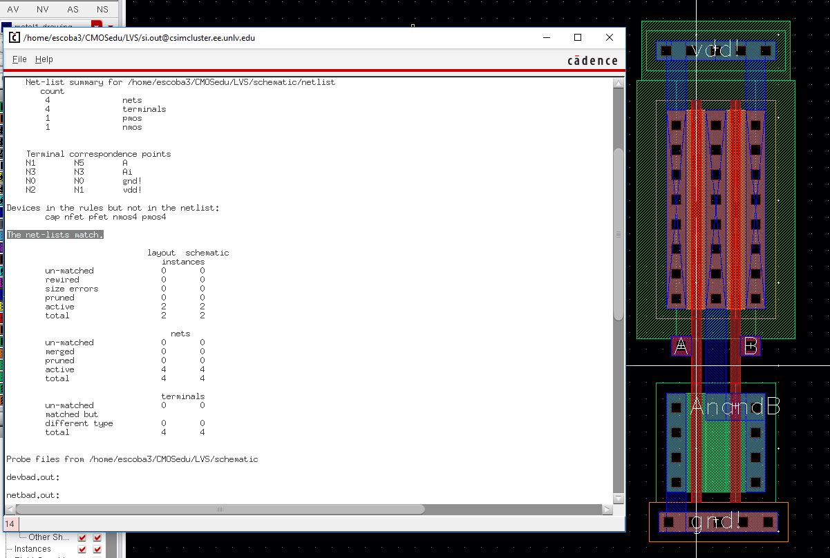 LVS layout - net lists match! |
 Notice that the W/L ratio is now 6u/.6u |  I also created a new symbol, only initials were added |
 A good way to start is to create a standard cell frame to place circuits on top off. | 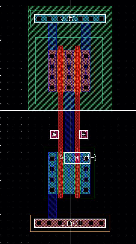 With the standard cell frame, we can create circuits faster. |  Passed LVS |
 XOR Schematic View |  XOR Symbol View |
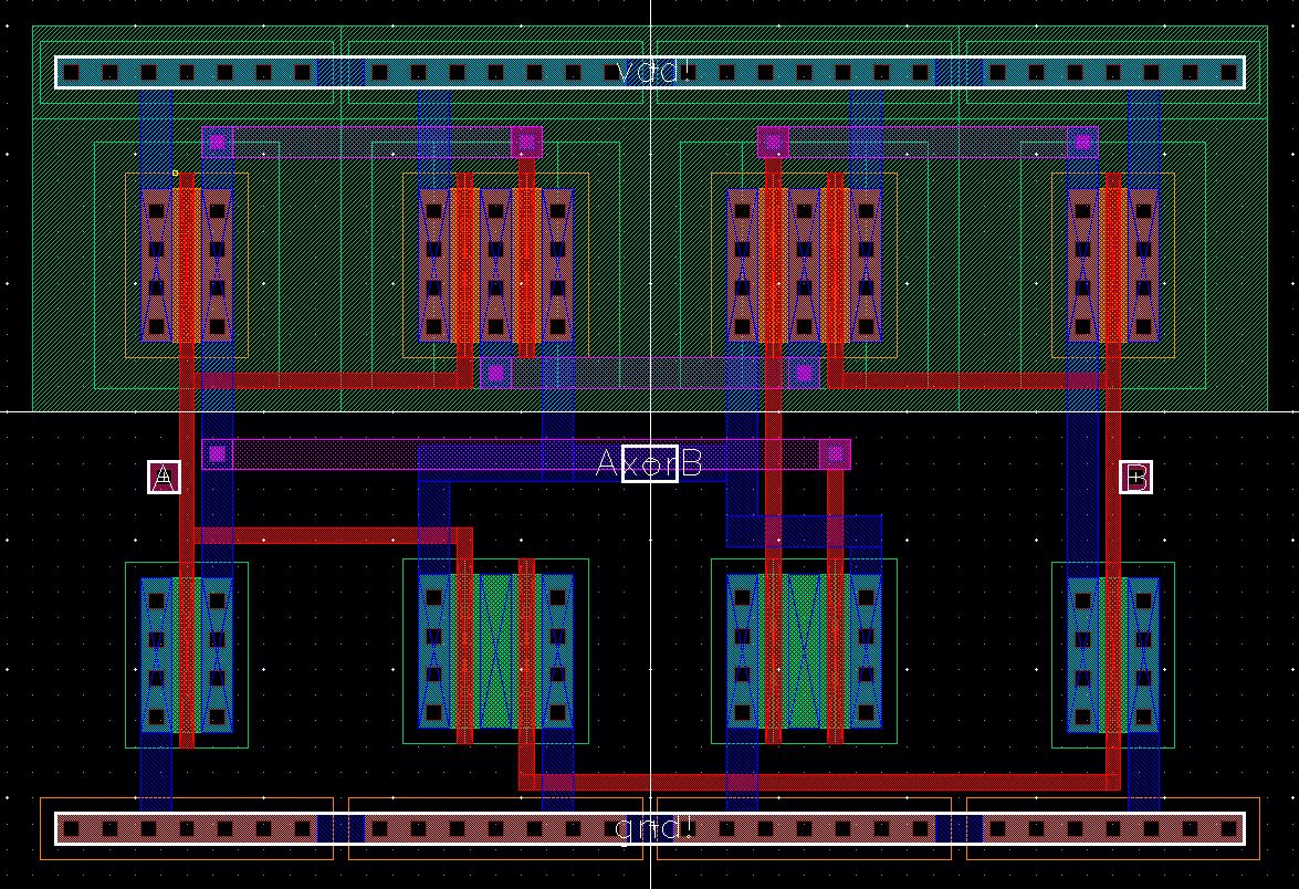 Layout of XOR Logic gate using standard cell frames | 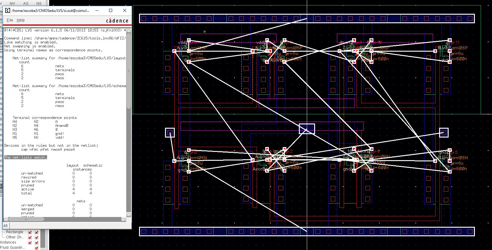 A passed LVS |
 Inverter, Nand, Xor Simulation Schematic | 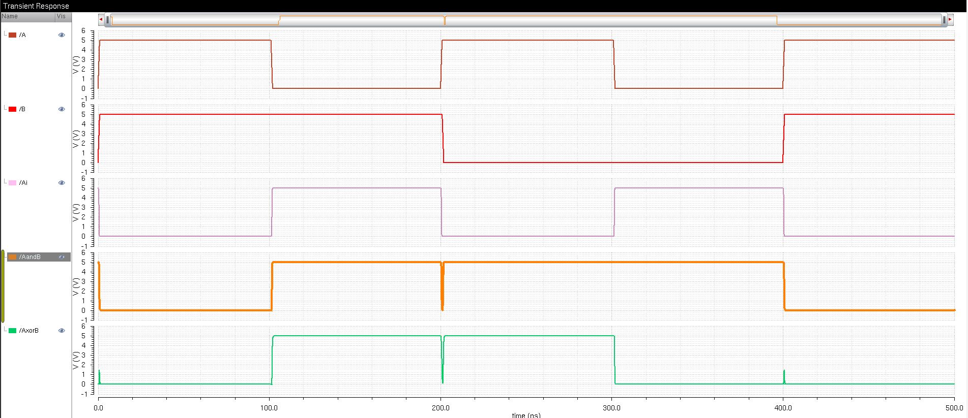 Simulation Results from Nand, Xor, and Inverter Schematic |
| A | B | Cin | S | Cout | |
| 0 | 0 | 0 | 0 | 0 | |
| 0 | 0 | 1 | 1 | 0 | |
| 0 | 1 | 0 | 1 | 0 | |
| 0 | 1 | 1 | 0 | 1 | |
| 1 | 0 | 0 | 1 | 0 | |
| 1 | 0 | 1 | 0 | 1 | |
| 1 | 1 | 0 | 0 | 1 | |
| 1 | 1 | 1 | 1 | 1 |
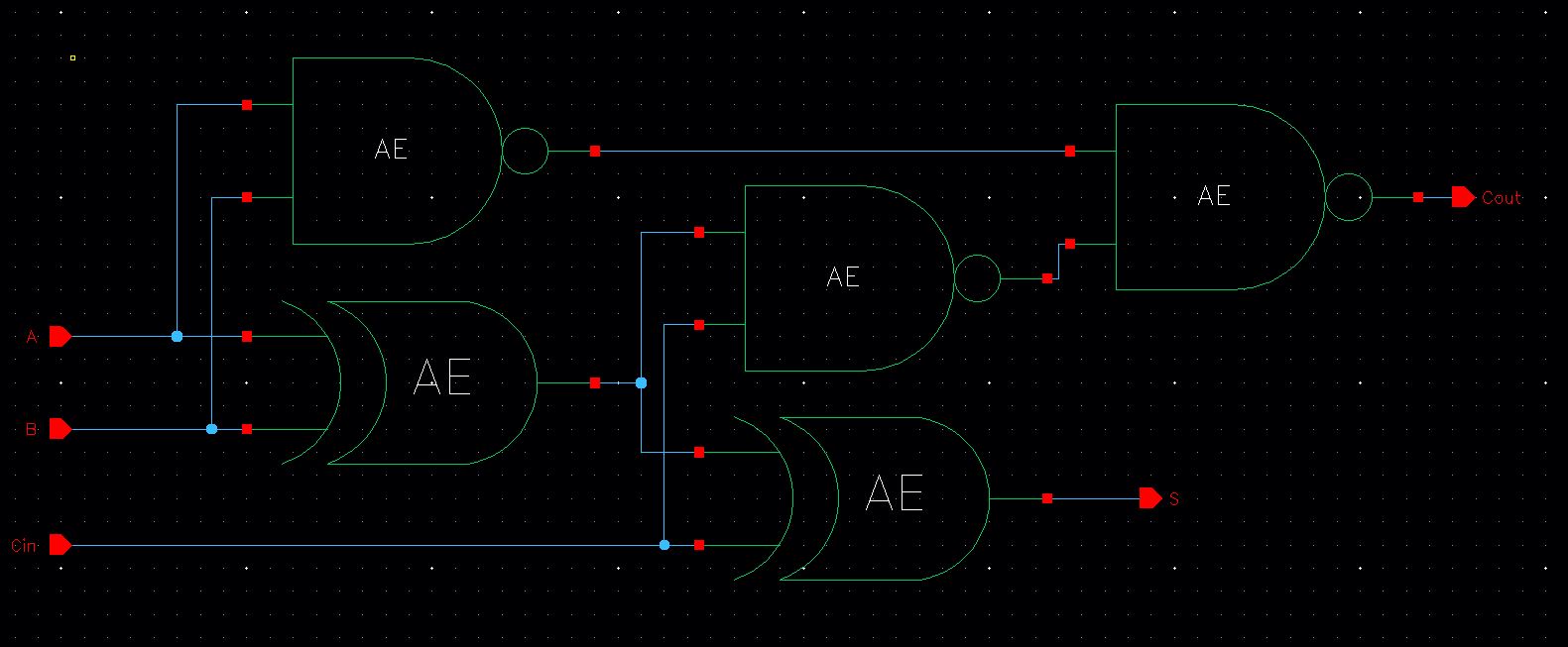 Full adder Schematic |  Full adder symbol |
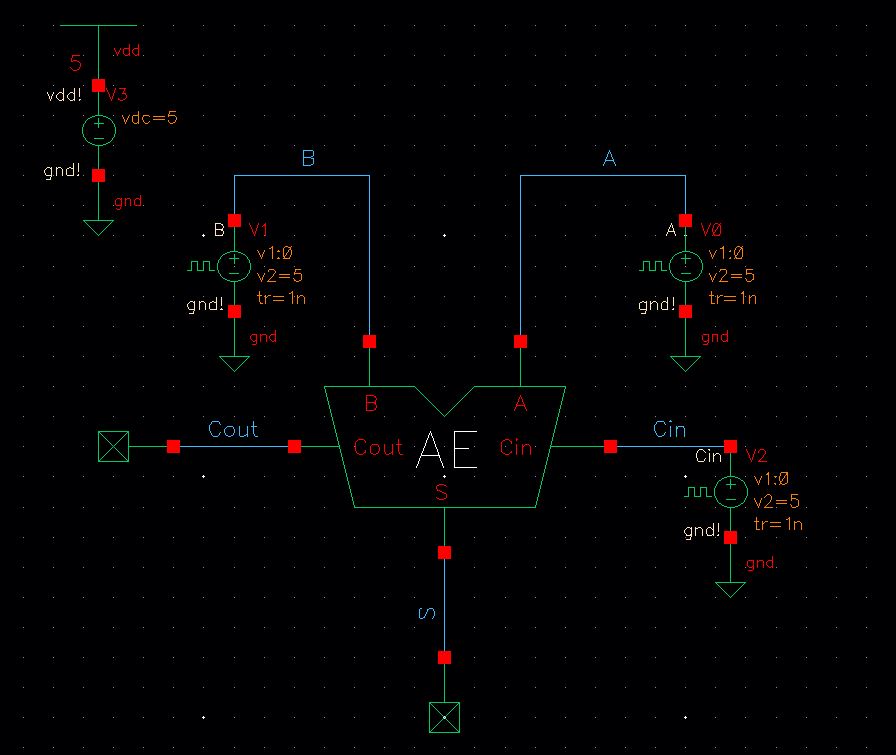 Full adder simulation schematic |  Full adder simulation results |
