Lab 2 - ECE 421L 

Author :: Aaron Escobedo

Escoba3@unlv.nevada.edu

September 13th, 2017

Pre-Lab

Once I was able to download the lab2.zip files and upload them to the proper directory, as well as defining the new directory, this is the schematic that first loaded

http://cmosedu.com/jbaker/courses/ee421L/f17/students/escoba3/Lab2/Schematic%201.JPG
Following that, I ran an ADE simulation to see the input voltage vs the output voltage, this following is what I found;

http://cmosedu.com/jbaker/courses/ee421L/f17/students/escoba3/Lab2/Output1.JPG
One of the pre-lab assignments asked us to solve for the least significant bit, of which there is a formula to assist us which is as follows;

http://cmosedu.com/jbaker/courses/ee421L/f17/students/escoba3/Lab2/lsb%20calculation.JPG
Since our Vref is 5V, and our N = 10, we should expect a LSB of ~4.88mV. When we change the input voltage to this value, we find this to be true.

http://cmosedu.com/jbaker/courses/ee421L/f17/students/escoba3/Lab2/Schematic2.JPG

http://cmosedu.com/jbaker/courses/ee421L/f17/students/escoba3/Lab2/Output2.JPG

Lab 2

Design of a 10-bit DAC using an n-well R of 10k

http://cmosedu.com/jbaker/courses/ee421L/f17/students/escoba3/Lab2/N_Well.JPG

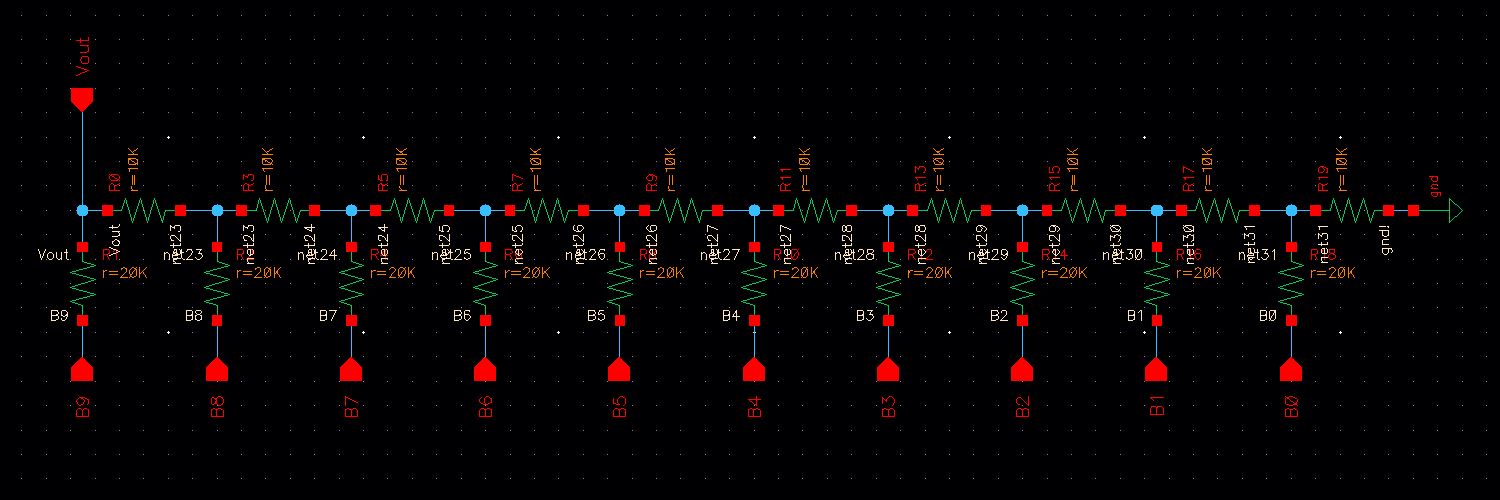
This design follows what was generally expected except I place a 2R valued resistor instead of 2 R sized resistors in series. 

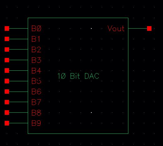
How to create a symbol view for your design

With the above n-well constructed, we can create a symbol to make it much easier to view in a large circuit. By selecting Create -->Cellview-->From Cellview, we should get something like this;

http://cmosedu.com/jbaker/courses/ee421L/f17/students/escoba3/Lab2/10bitDAC.JPG

Determining the total output resistance of the DAC

When two resistors are placed in parallel of the same value, the result will be a new total resistance of half the orginal. This idea actually works itself here as the last two resistors are 2R//2R, which would equal R. That R is in series with another R, thus again creating a 2R. This process repeats which results in the final output resistance being R alone. 

Delay, driving a load. 

If we use the formula 0.7RC to predict the delay of a DAC in this manner, we should expect the following;
R = 10kl
C = 10pF
0.7(10k)(10p) = 70ns

The following represents my schematic and simulation of this idea;

http://cmosedu.com/jbaker/courses/ee421L/f17/students/escoba3/Lab2/Schematic3.JPG

http://cmosedu.com/jbaker/courses/ee421L/f17/students/escoba3/Lab2/Output3.JPG

As expected, the first time constant is acheived at ~70ns

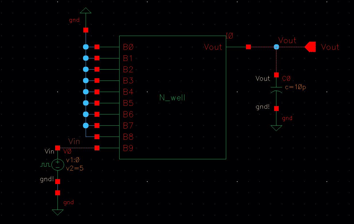
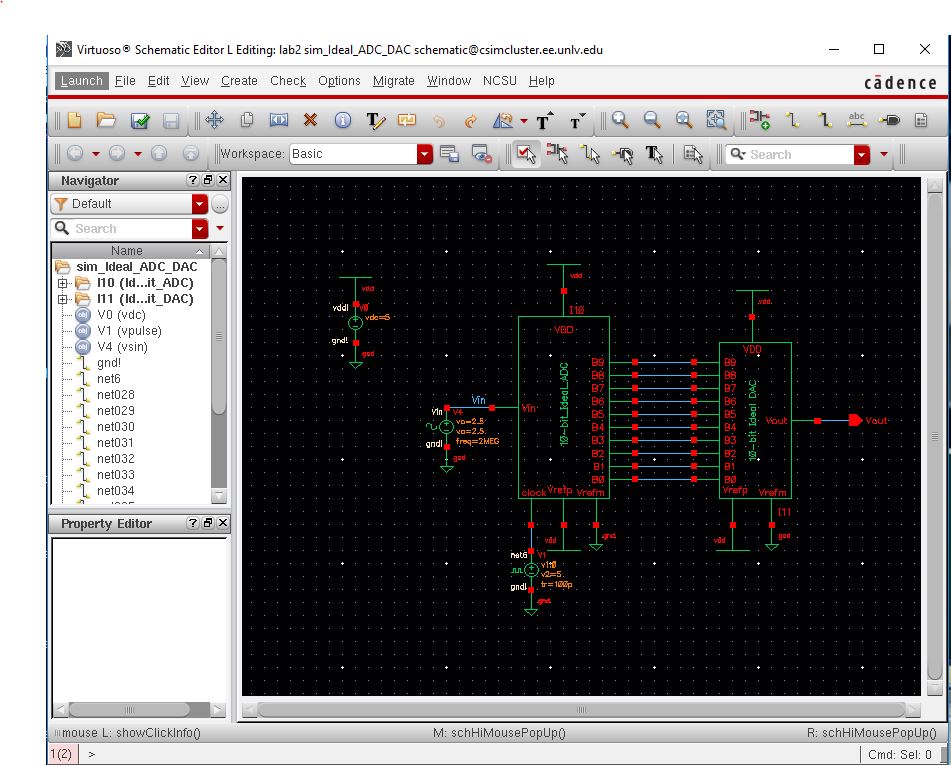
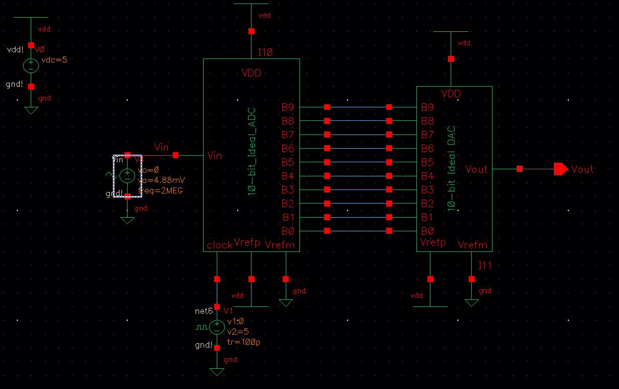
Simulations to verify your design functions correctly

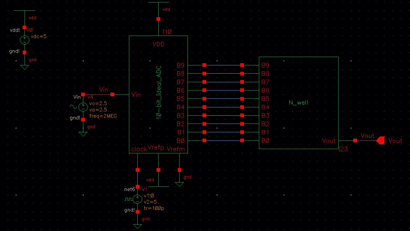
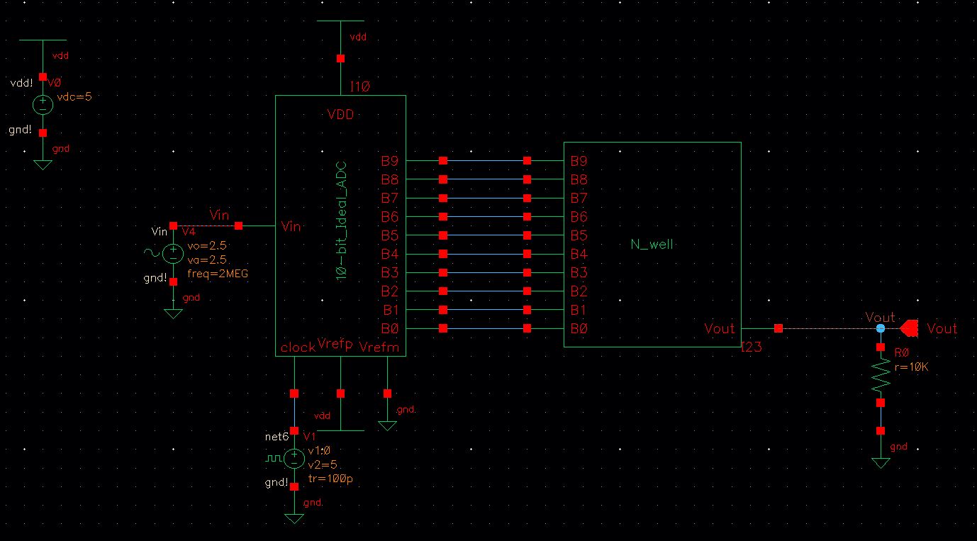
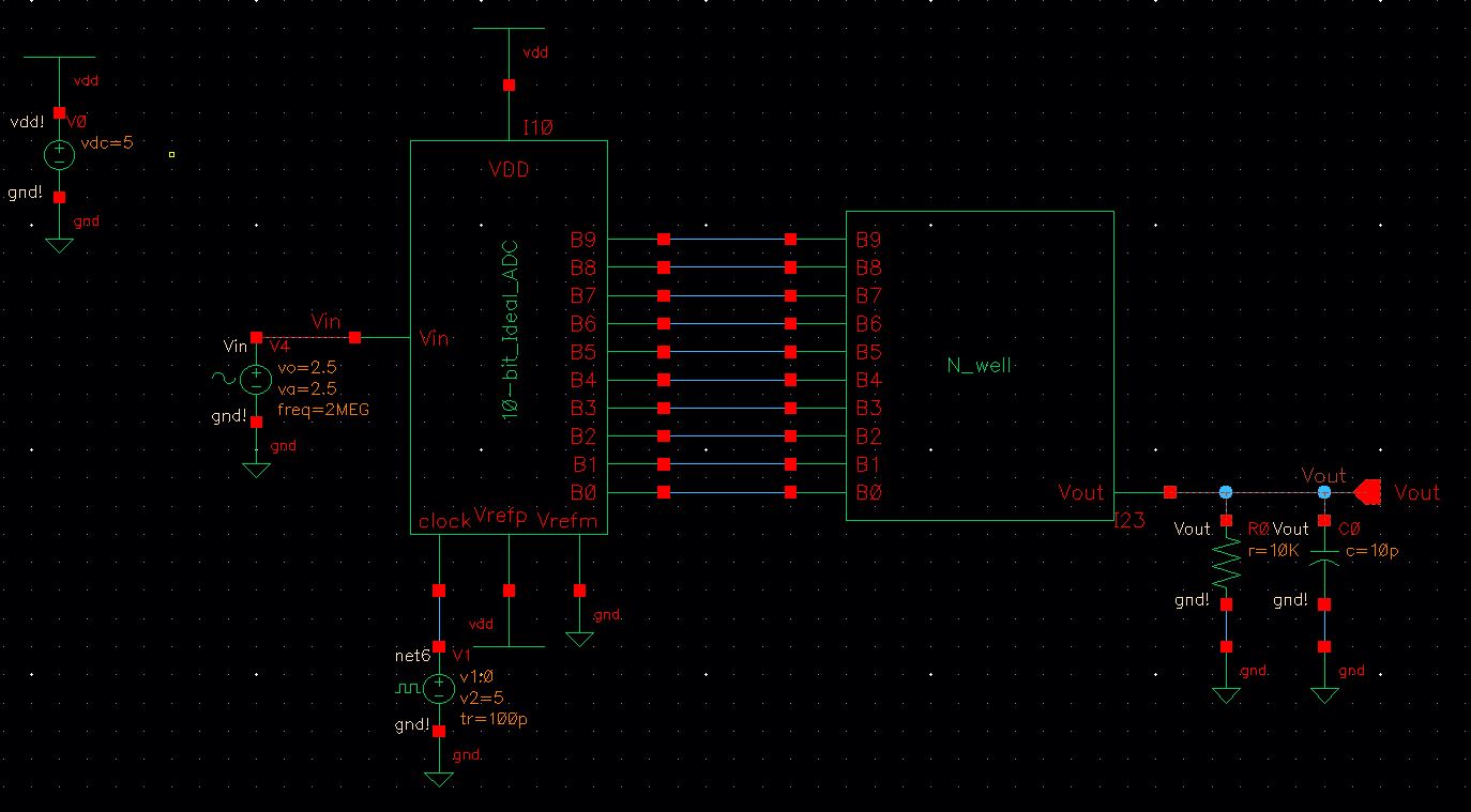
Now, I will use the DAC I recreated to replace the Ideal DAC in the orginal schematic, below represents my new schematic

http://cmosedu.com/jbaker/courses/ee421L/f17/students/escoba3/Lab2/Schematic4.JPG

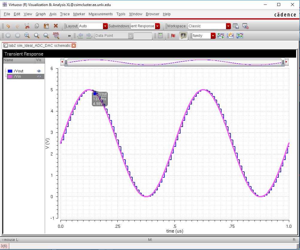
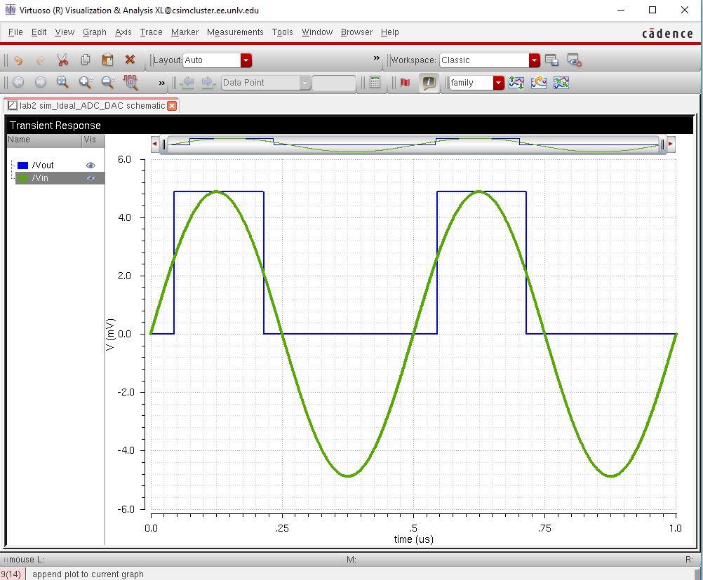
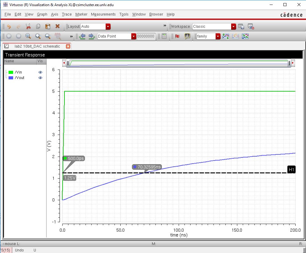
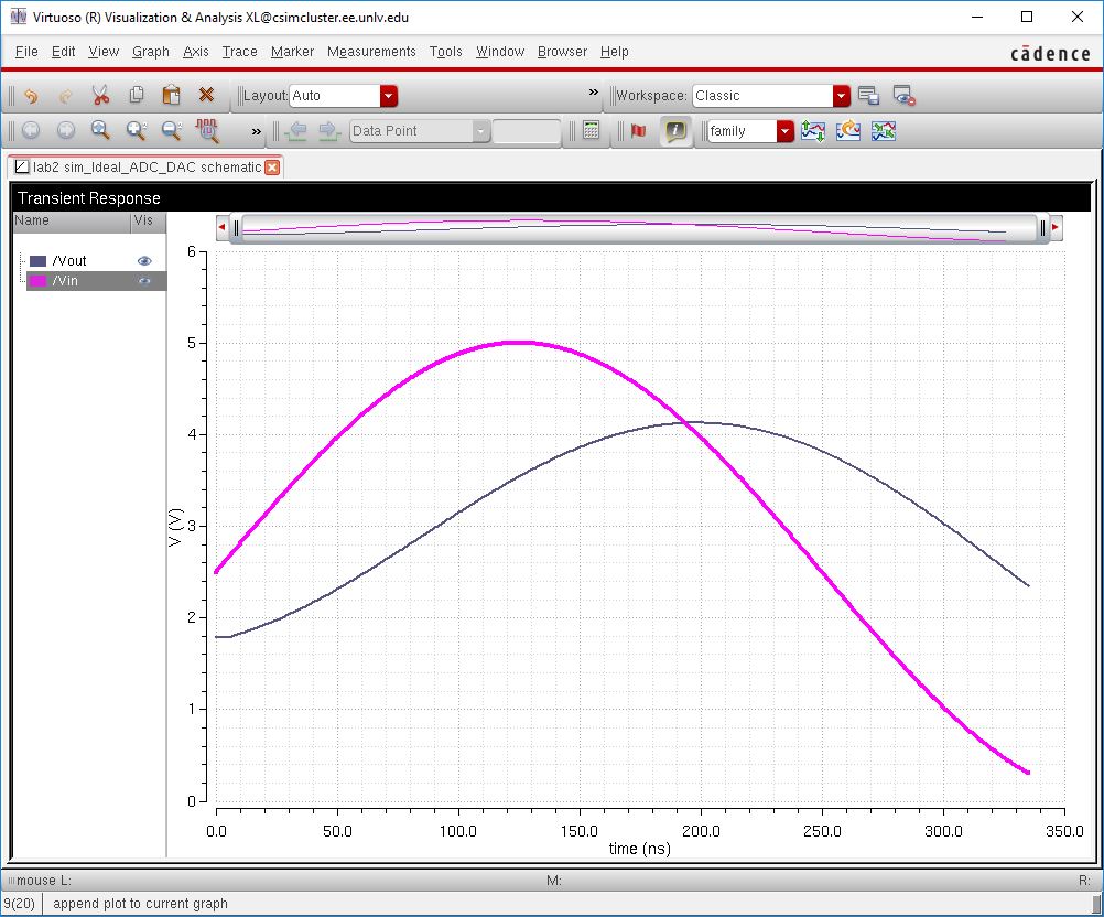
When I simulate this, I received the following

http://cmosedu.com/jbaker/courses/ee421L/f17/students/escoba3/Lab2/Output4.JPG

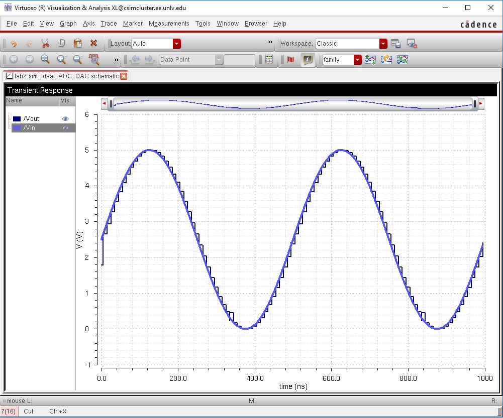
Which nearly represents what we saw with the ideal DAC, the difference being a start up time in the beginning of the output signal

Simulation when driving a 10k load

http://cmosedu.com/jbaker/courses/ee421L/f17/students/escoba3/Lab2/Schematic5.JPG

http://cmosedu.com/jbaker/courses/ee421L/f17/students/escoba3/Lab2/Output5.JPG

Explain what happens when driving a 10k Load

We can clearly see that the output voltage is reduced, while all other factors remain the same

Simulation with a 10pF Load

http://cmosedu.com/jbaker/courses/ee421L/f17/students/escoba3/Lab2/Schematic6.JPG

http://cmosedu.com/jbaker/courses/ee421L/f17/students/escoba3/Lab2/Output6.JPG

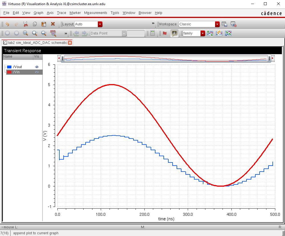
With this, we can clearly see a phase shift in the output voltage

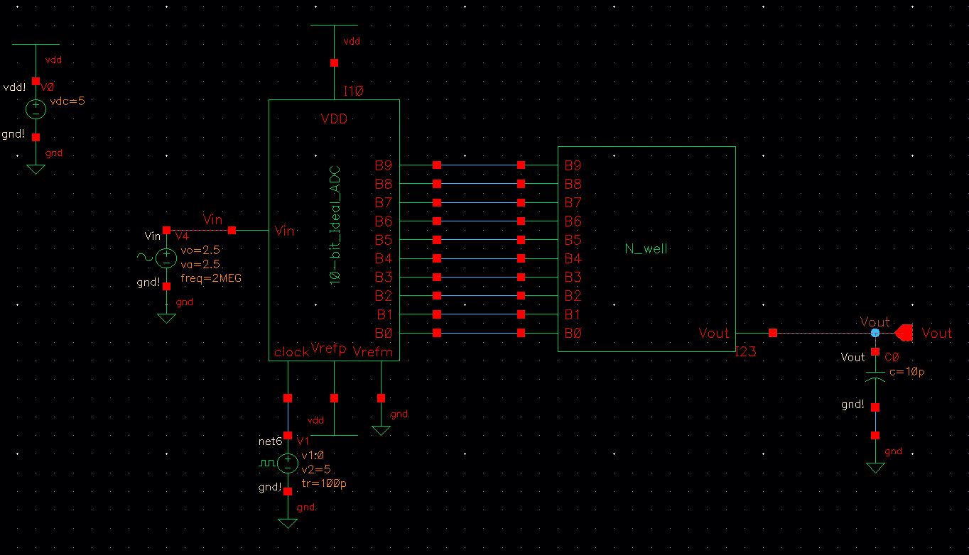
Simulation with an RC Load

http://cmosedu.com/jbaker/courses/ee421L/f17/students/escoba3/Lab2/Schematic7.JPG

http://cmosedu.com/jbaker/courses/ee421L/f17/students/escoba3/Lab2/Output7.JPG

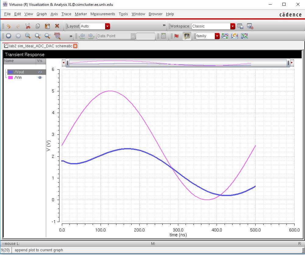
With this, we can see both a phase shift and a reduction in output voltage

Real Circuit considerations

In a real circuit, the resistance of the switches may not be small compared to the value of R, in such a case, the voltage on the output will be smaller as the resistance in series will be taken up more by the input resistance. 

Backing up files

http://cmosedu.com/jbaker/courses/ee421L/f17/students/escoba3/Lab2/Backup1.JPG

http://cmosedu.com/jbaker/courses/ee421L/f17/students/escoba3/Lab2/Backup2.JPG


Return to Students