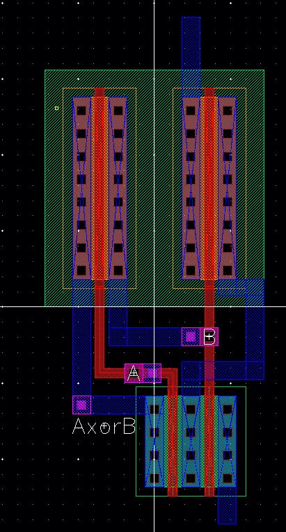
XOR Layout
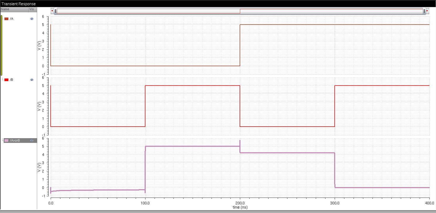
XOR No Load Sim
Final Project - ECE 421L
XOR Layout | XOR No Load Sim |
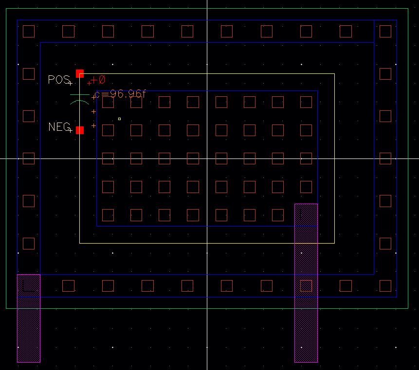 96.96 fF Capacitor Extracted | 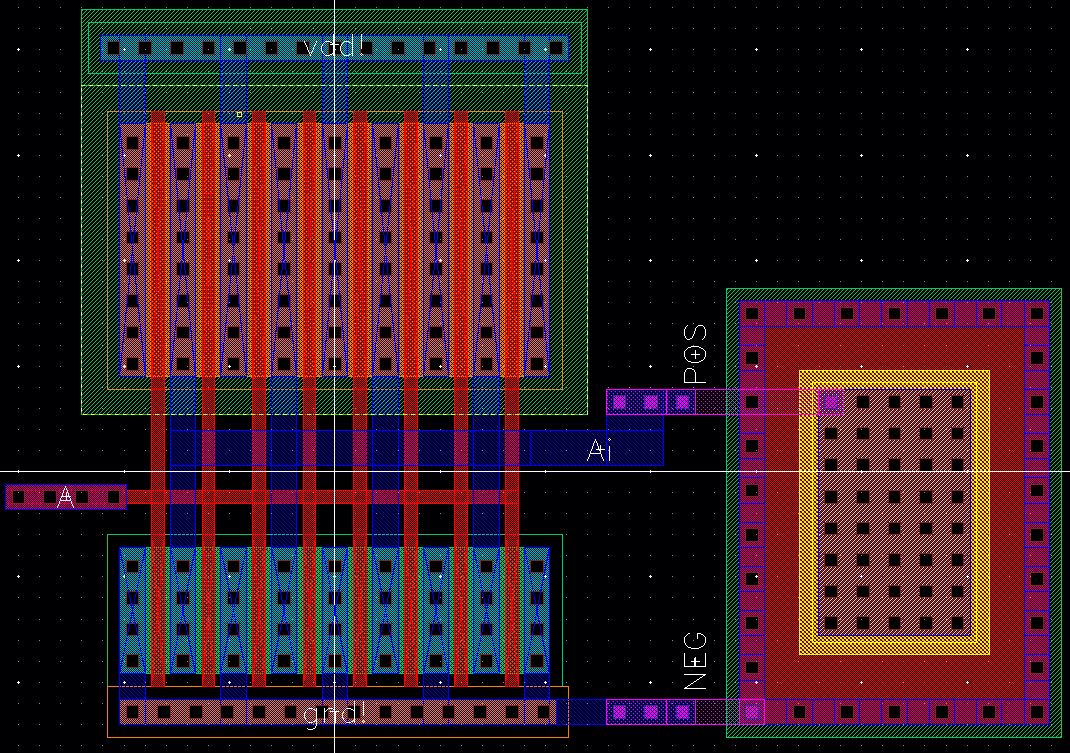 Buffer Layout with Capacitor |
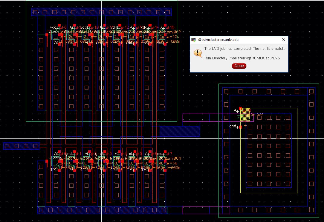 Buffer Extracted View with LVS | 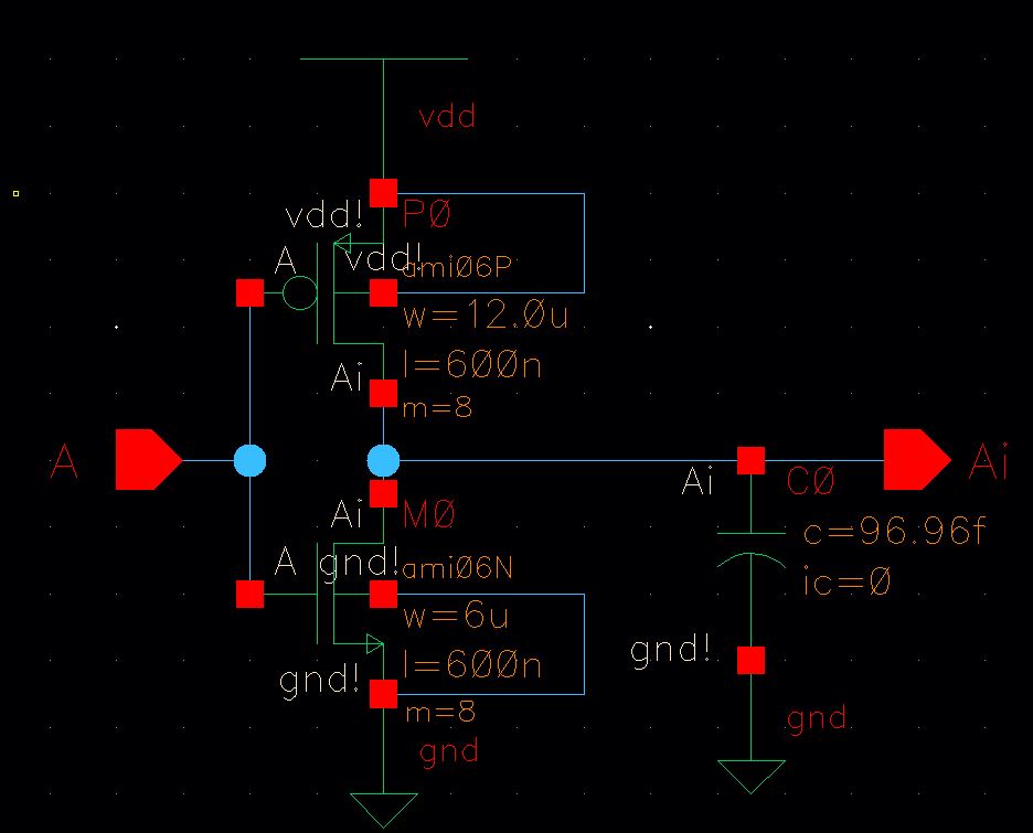 Buffer Schematic |
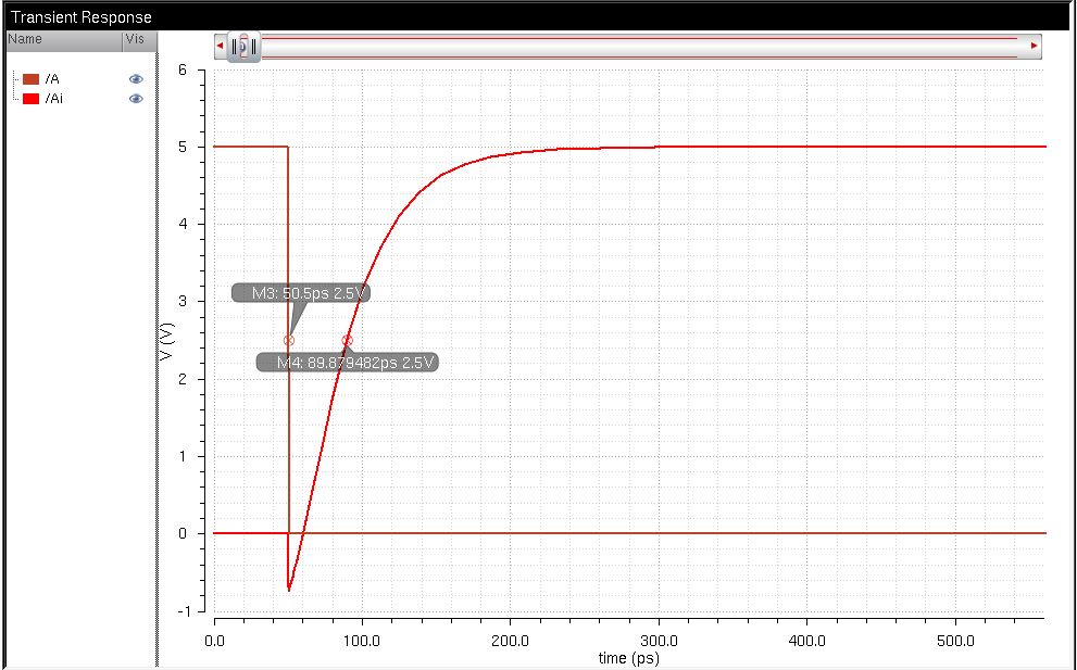 Buffer Delay |
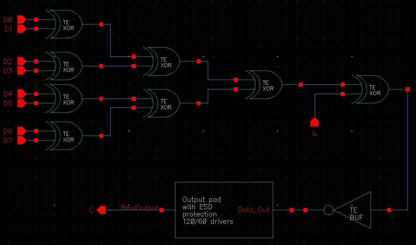
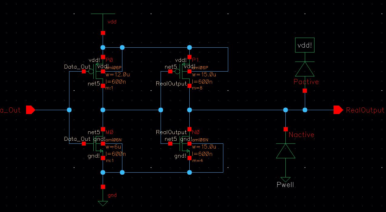 Output Pad with ESD protection |
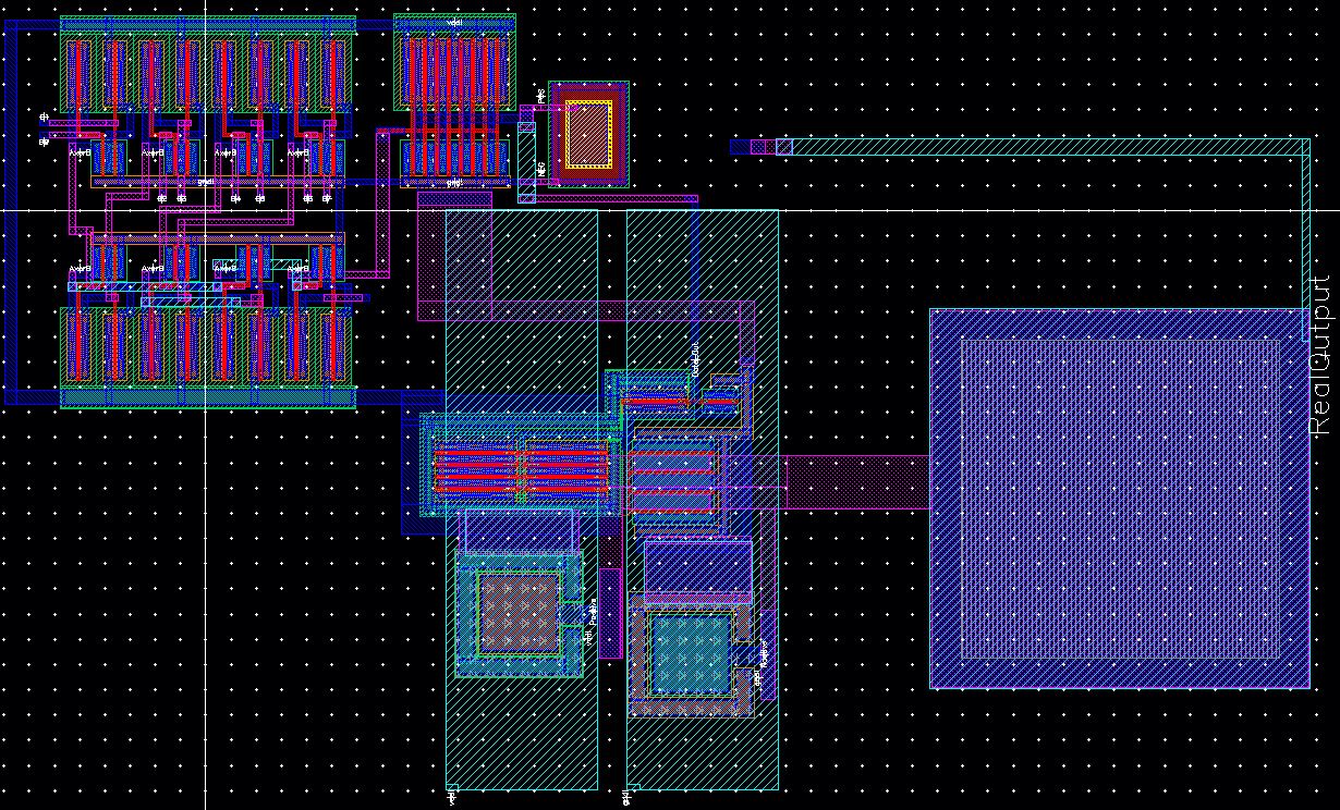 Even Parity Full Layout | 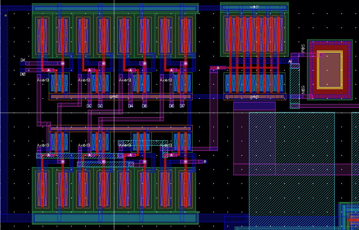 Even Parity Layout Zoom |
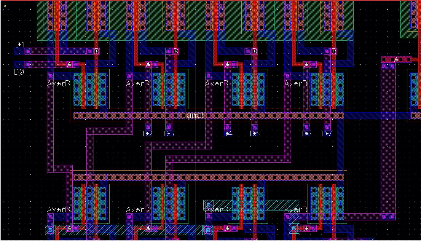 Even Parity Gate Connection Zoom | 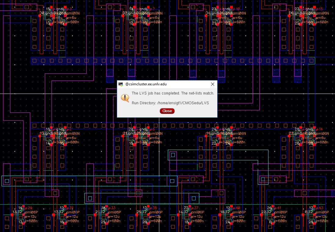 Even Parity Extracted View with LVS |
 Even Parity Schematic | 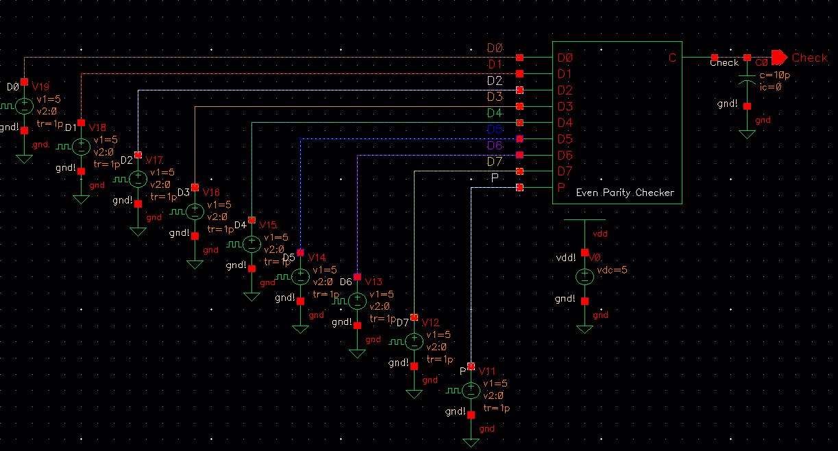 Even Parity Simulation Schematic with Scope Capacitor |
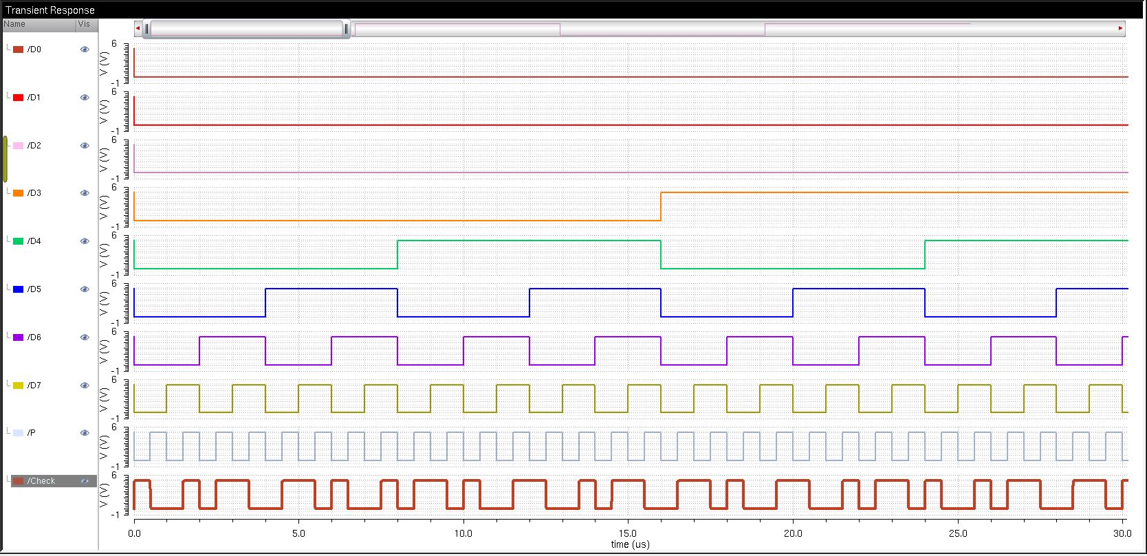 1MHz Simulation with No Scope Load | 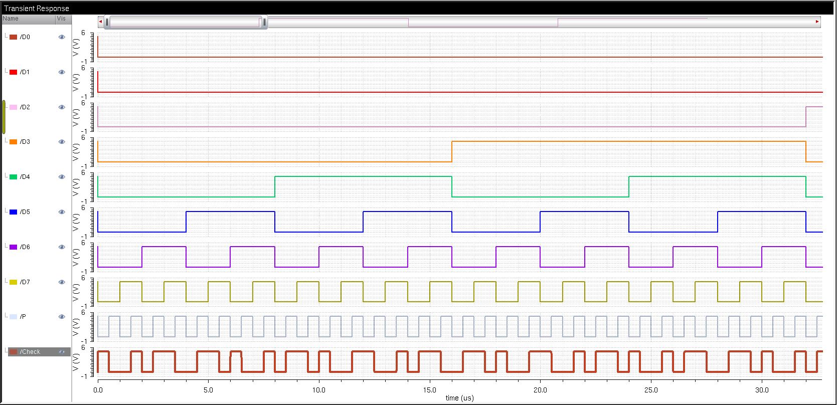 1MHz Simulation with Scope Load |