Lab 3 - EE 421L
Authored by Trevor Ensign
ensigt1@unlv.nevada.edu
September 20, 2017
Pre-Lab Work
For
the pre-lab, all of my previous work was backed up to my Google drive,
and Tutorial 1 was completed. This involved creating a layout10K n-well
resistor and resistor voltage divider. The results of this can be seen
below.
Lab Work
For
this lab, a layout for the 10-bit DAC from lab 2 was constructed. The
first step was to create a n-well 10K resistor layout to be used in the
design. The height of the design was set to the minimum of 3.6 micro to
match the height of a 1 column/row ntap connection. Because of the
minimum interval of .15, the width could not be set to the exact
dimenisions needed for 10K. However, the value obtained in the
extracted view is close enough to 10K to not effect the results. The
resistor has final dimensions of 3.6 micro by 44.1 micro, with a value
of 10.03K. A picture of the extracted view with the resistor value can
be seen below.
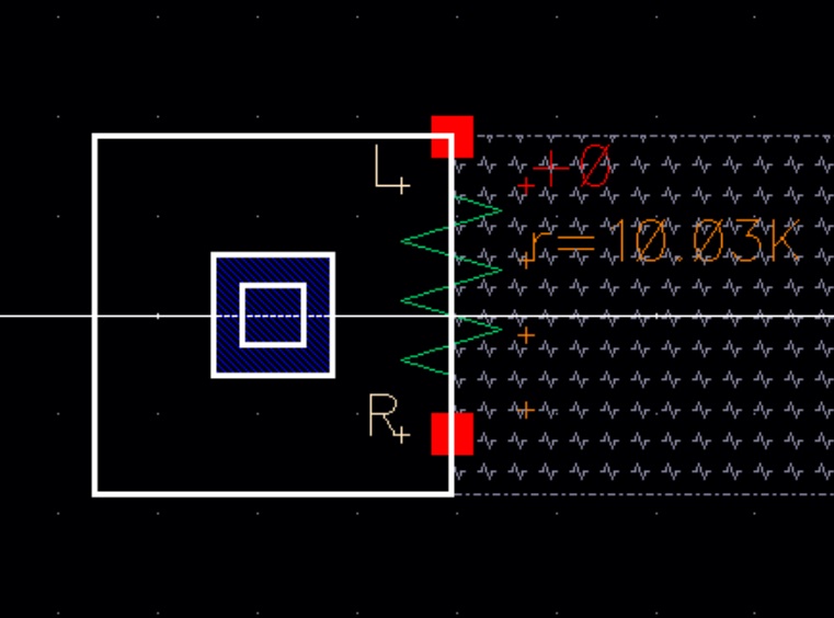
Resistor Extracted View
Using this 10K resistor, the DAC layout was created. Each resistor has the same X value and varying Y values to create a stacked
view of the resistors. After wiring the resistors to match the 2R-R
branch from the lab 2 DAC circuit design, each 2R-R branch was cascaded
to create the full DAC. Pins were added for each bit, Vout, and ground
to match the lab 2 DAC schematic. After completed, a DRC was run to check for errors. Since there were no errors, the layout was extracted and a LVS was
executed between the extracted view and lab 2 schematic. Below are
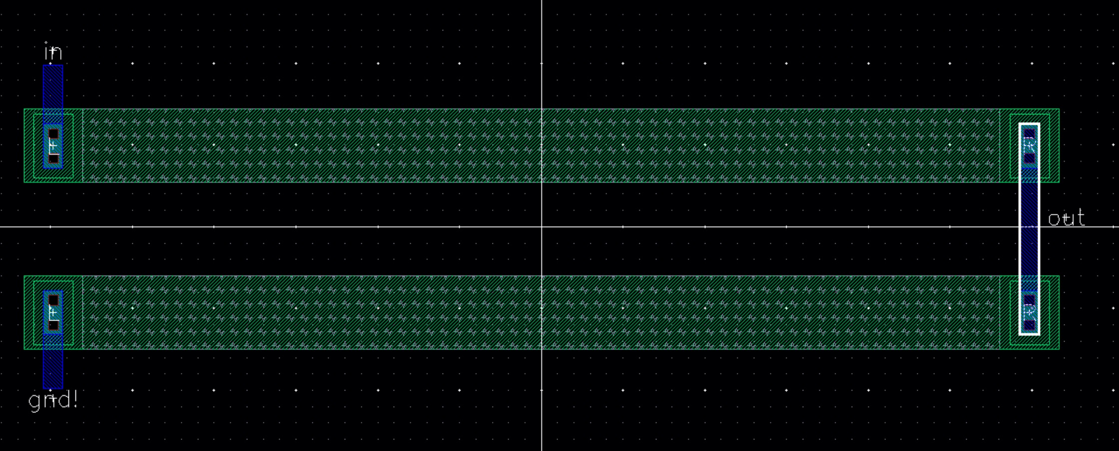
images of the LSB of the DAC layout, DRC and LVS results.
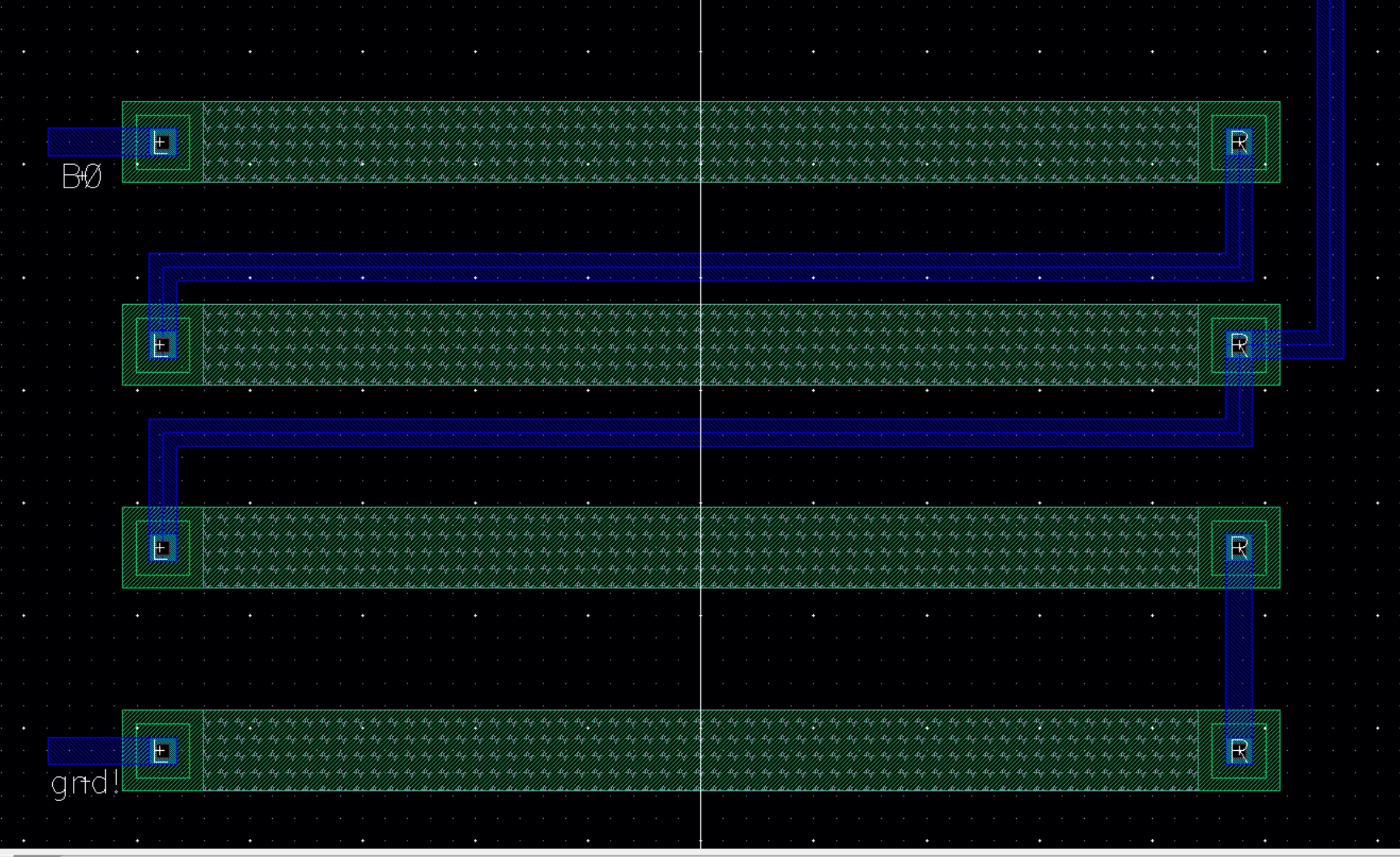
Least Significant Bit DAC Layout
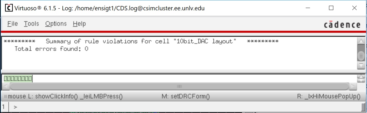
DRC Results | 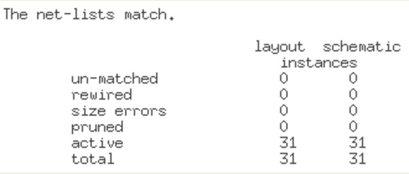
LVS Results |
You can download files for this lab here.
Return to Trevor's Labs
Return to EE 421L Labs