Lab 8 -
EE 421L
Reiner Dizon, dizonr1@unlv.nevada.edu
Angel Solis, solisa1@unlv.nevada.edu
John Dye, dyej1@unlv.nevada.edu
Today's
date is December 6, 2017
Lab
description: This
lab is about the generation of test chip layout for submission to MOSIS for fabrication.
DESIGN DIRECTORY:
Chip1_f17.zip
CHIP CONTENTS
- 31-stage ring oscillator with a buffer capable of driving an
off chip 20pF load
- NAND gate using 6/0.6 NMOS and PMOSs
- NOR gate using 6/0.6 NMOS and PMOSs
- XOR gate using 6/0.6 NMOS and PMOSs
- Inverter made with a 6u/0.6 NMOS and 12u/0.6u PMOS
- 6u/0.6u 4-terminal PMOS transistor
- 6u/0.6u 4-terminal NMOS transistor
- 25k-10k voltage divider
- Even Parity Checker Circuit
CHIP SCHEMATIC
CHIP LAYOUT
PIN CONNECTIONS
Ring Oscillator
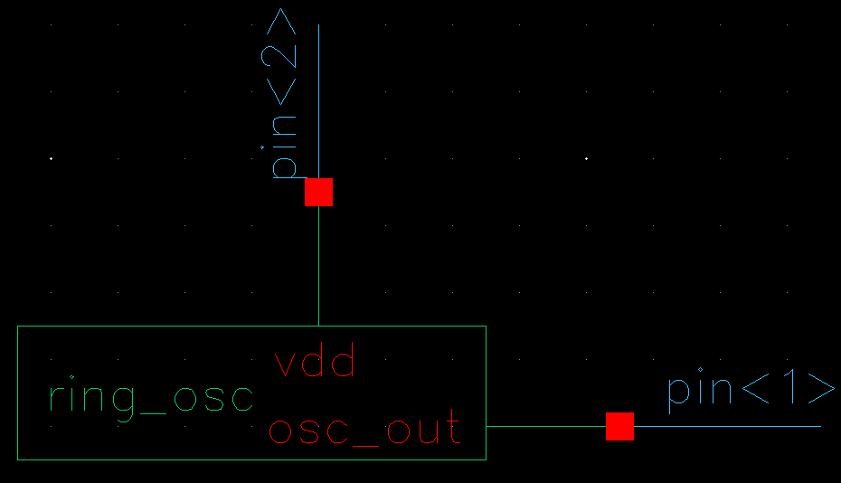 | | Pin | Connection | | Pin<1> | VDD | | Pin<2> | osc_out |
|
NAND Gate
 | | Pin | Connection | | Pin<21> | VDD | | Pin<22> | A | | Pin<23> | B | | Pin<24> | AnandB |
|
NOR Gate
 | | Pin | Connection | | Pin<36> | AnorB | | Pin<37> | B | | Pin<38> | A | | Pin<39> | VDD |
|
XOR Gate
 | | Pin | Connection | | Pin<3> | AxorB | | Pin<4> | B | | Pin<5> | A | | Pin<6> | VDD |
|
Inverter Gate
 | | Pin | Connection | | Pin<14> | VDD | | Pin<15> | In | | Pin<16> | Out |
|
PMOS Transistor
 | | Pin | Connection | | Pin<10> | Source | | Pin<11> | Gate | | Pin<12> | Drain | | Pin<13> | Body |
|
NMOS Transistor
 | | Pin | Connection | | Pin<7> | Drain | | Pin<8> | Gate | | Pin<9> | Source | | Pin<20> | Body (gnd!) |
|
Resistive Divider
 | | Pin | Connection | | Pin<17> | 25K in | | Pin<18> | 25K to 10K | | Pin<19> | 10K in |
|
Even Parity Checker Circuit
 | | Pin | Connection | | Pin<25> | D0 | | Pin<26> | D1 | | Pin<27> | D2 | | Pin<28> | D3 | | Pin<29> | D4 | | Pin<30> | D5 | | Pin<31> | D6 | | Pin<32> | D7 | | Pin<33> | P | | Pin<34> | check | | Pin<35> | VDD |
|
Return
to John's Labs
Return
to EE 421L Labs

