Lab 7 - ECE 421L
Authored
by John Dye (dyej1@unlv.nevada.edu),
November 9, 2017
Lab
description:
In
this lab, we instantiated arrays of logic gates to show the use of
buses, as well as design and layout a full 8-bit adder. At the end of
the lab, we have all of the building blocks necessary to building an
ALU.
Prelab:
All of the previous lab material has been backed up in Google Drive.
Lab Report:
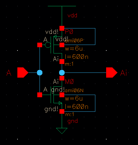
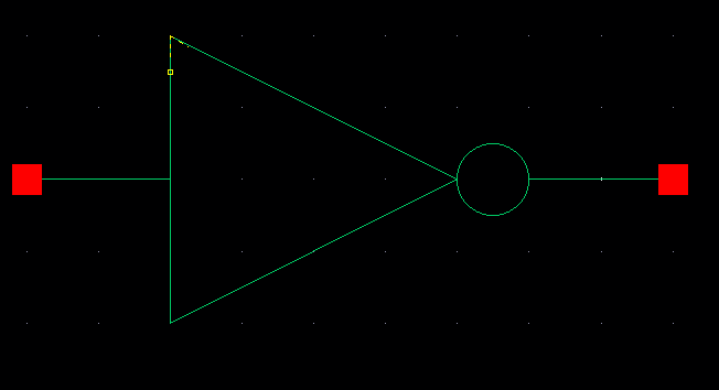
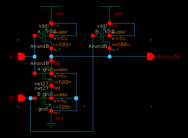
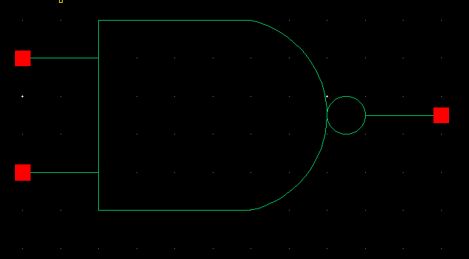
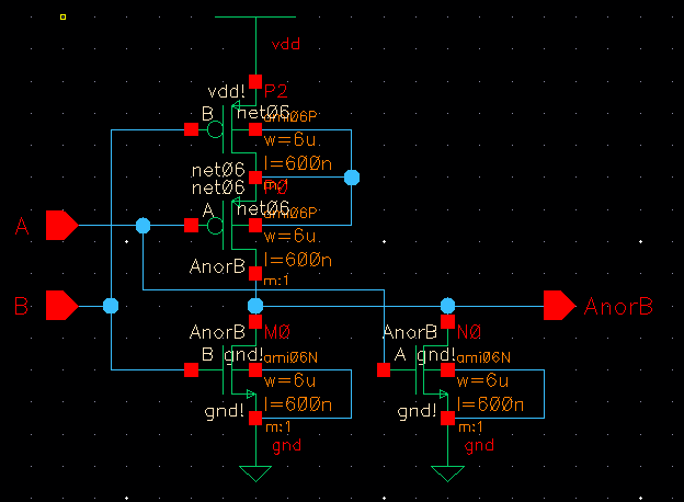
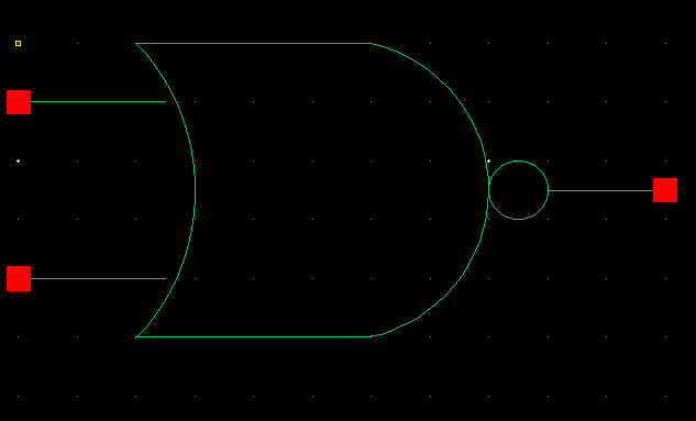
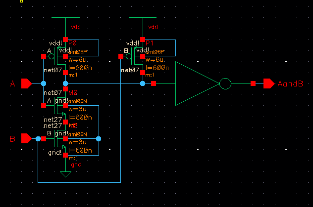
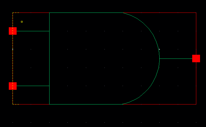
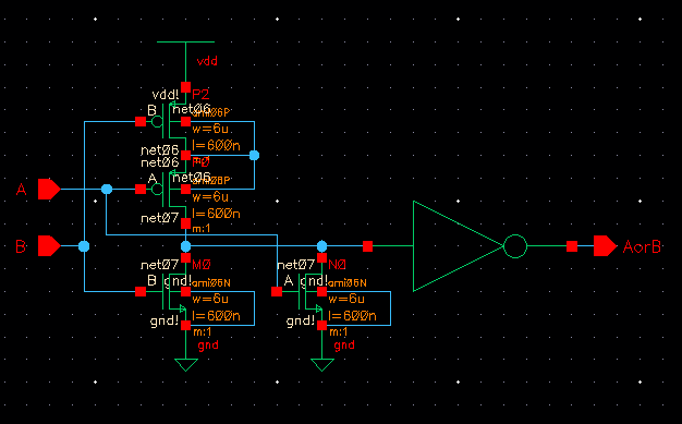
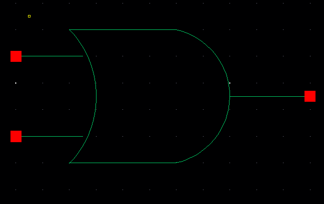
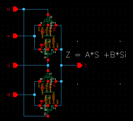
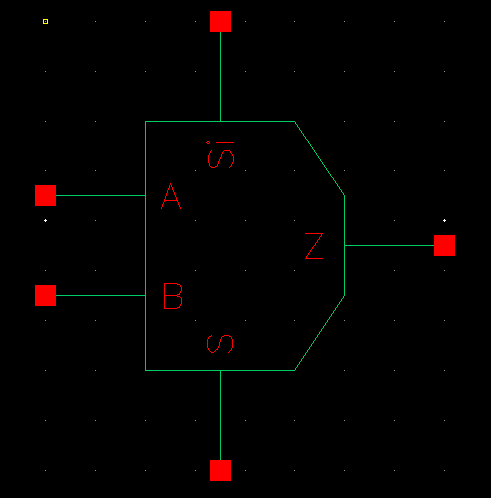
To begin, shown below are the schematic and symbol for some of the basic logic gates that will be used within this lab,
Next,
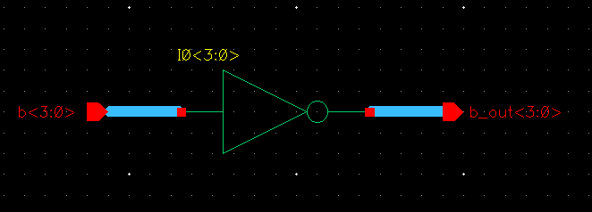
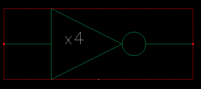
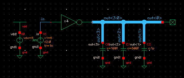
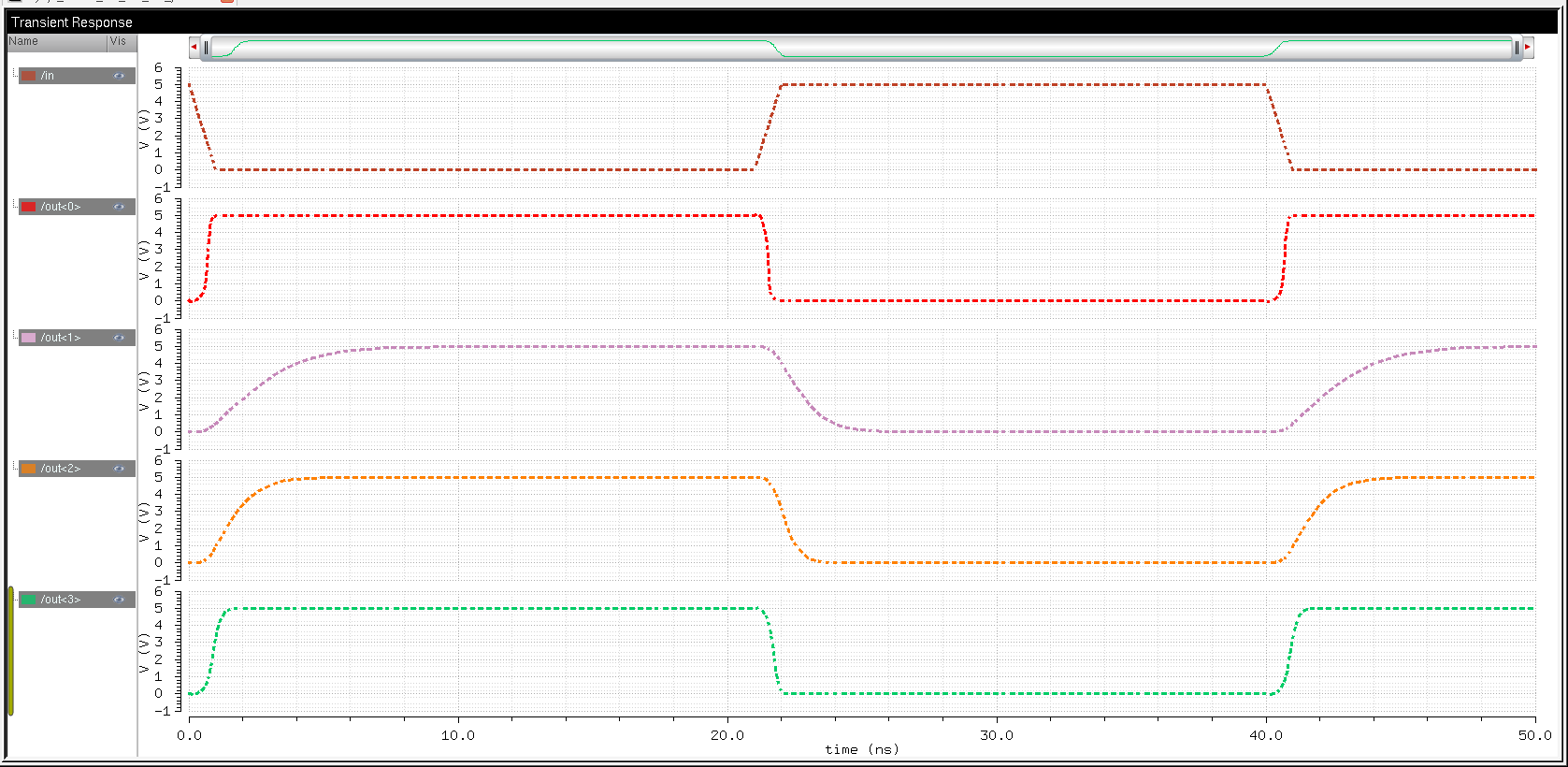
a 4-bit array of inverters was created. Shown below are the schematic,
symbol, simulation schematic, and simulation results for the inverter
circuit,
Next,
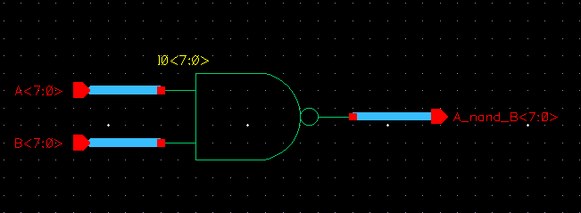
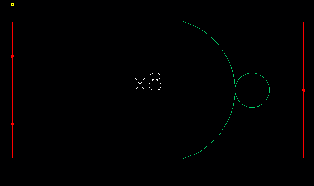
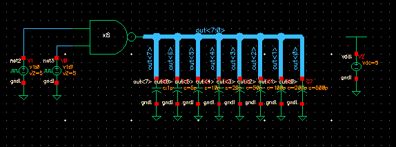
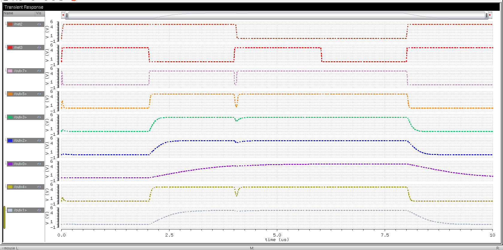
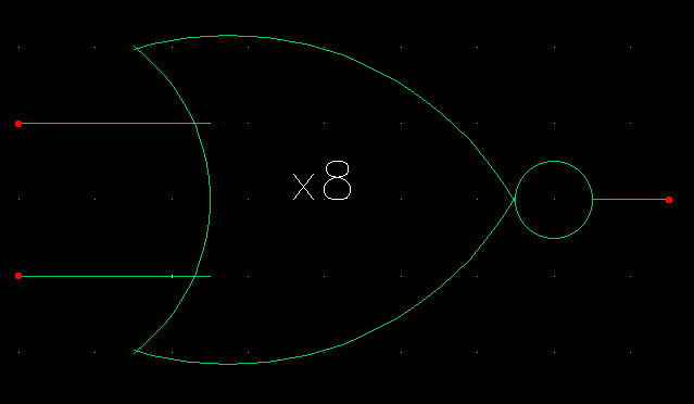
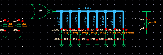
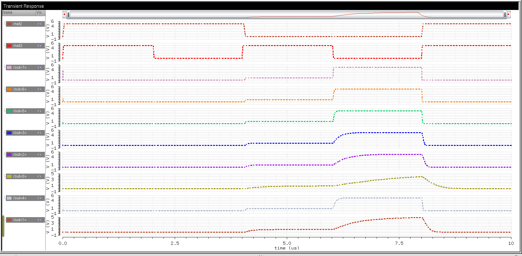
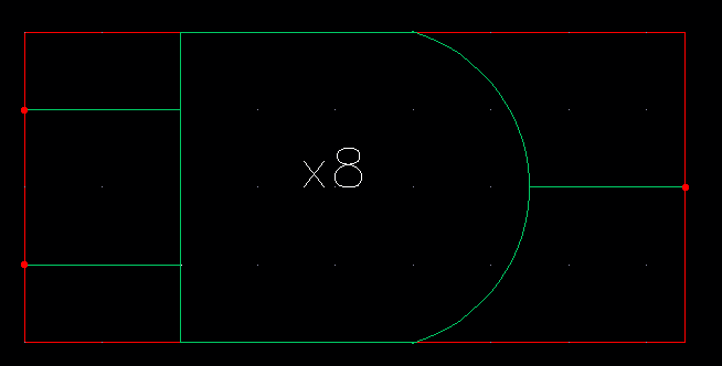
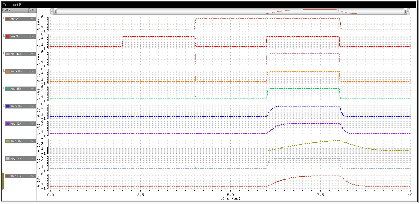
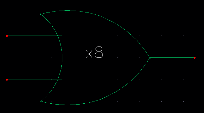
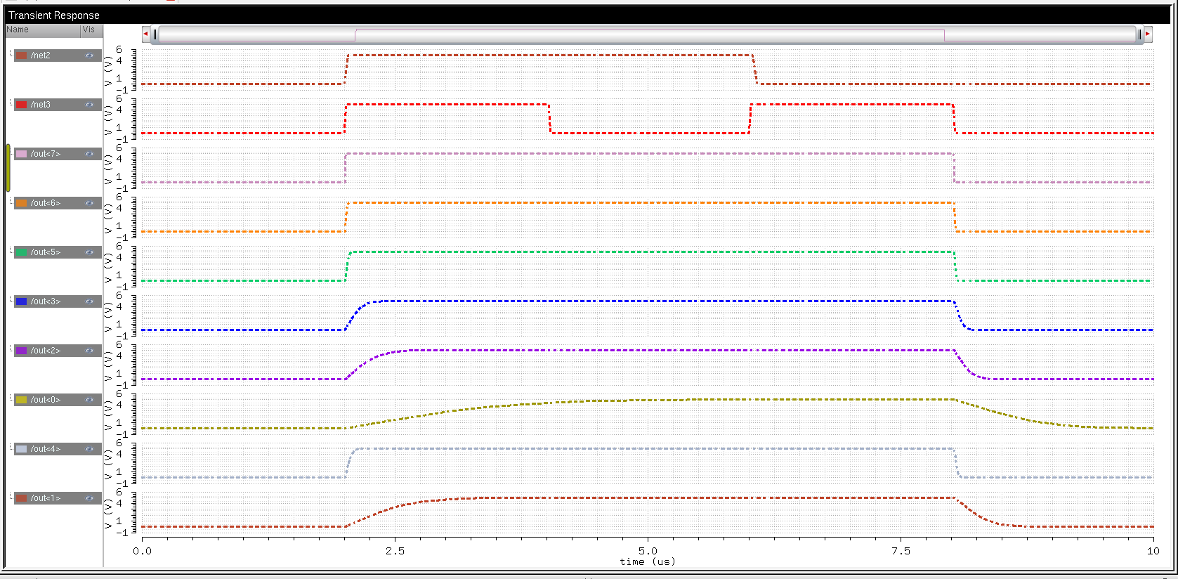
4-bit arrays were created for NAND, NOR, AND, and OR. Because of
spacing issues, some of the photos are small and hard to see. If you
have this issue, please click on the picture to see and enlarged image.
Shown below are the schematic, symbol, simulation schematic, and
simulation results for the circuits,





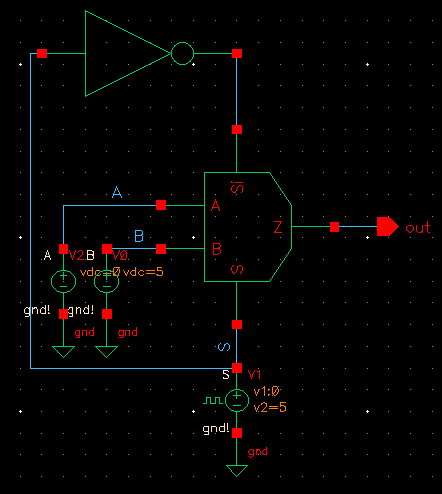
Then, I simulated the provided 2-1 MUX using the simulation schematic and results shown below,
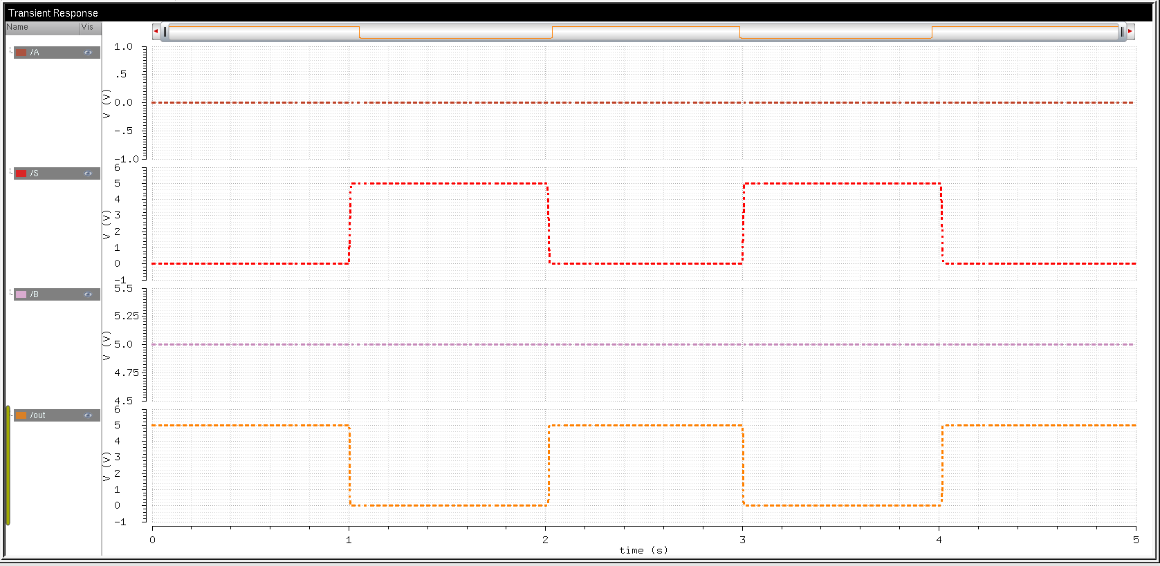
As
can be seen from the schematic, A =0 and B=1. When S=0, out = B, and
when S=1, out=A. So, S is used to select which of the inputs will be
connected to the output. What is simulated above is the multiplexing
operation. To demultiplex, simply make the "out" put your input, and
make the "A" and "B" pins your outputs. All that the multiplexer
circuit does is select which outputs and inputs are connected together,
so nothing else needs to be changed, so the simulation above also works
for demultiplexing.
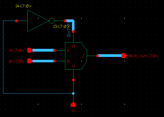
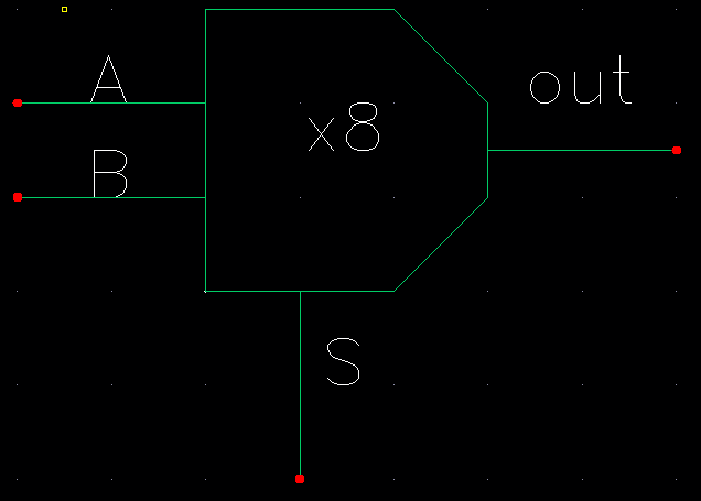
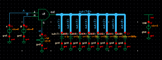
Next, an 8-bit bus 2-1 multiplexer was created, as shown below,
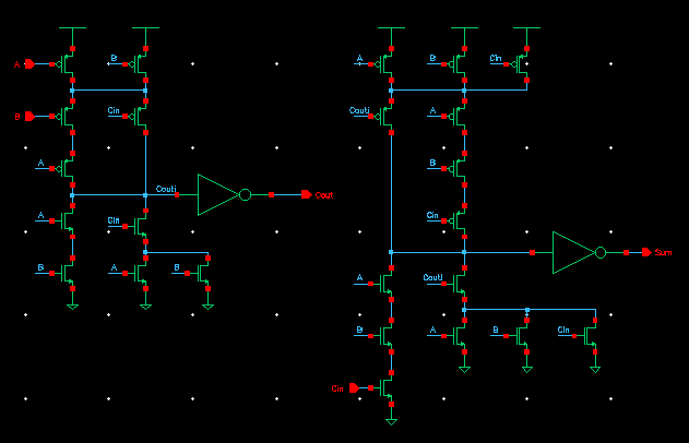
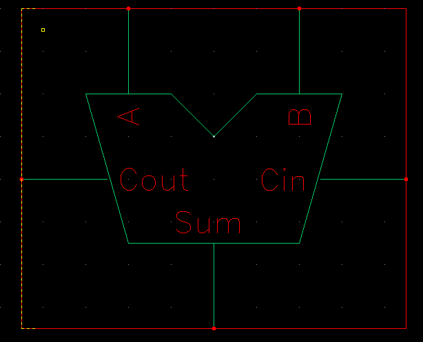
Shown below is the schematic and symbol for a single full-adder,
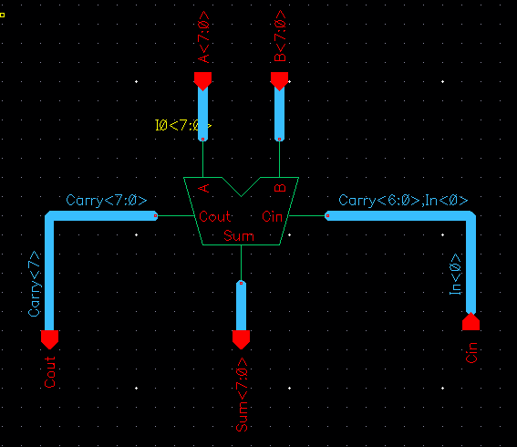
Next, an 8-bit array of adders was created. Shown below are the schematic and symbol,
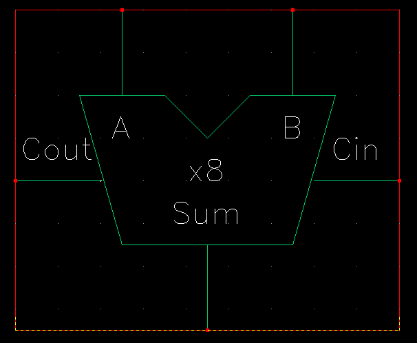
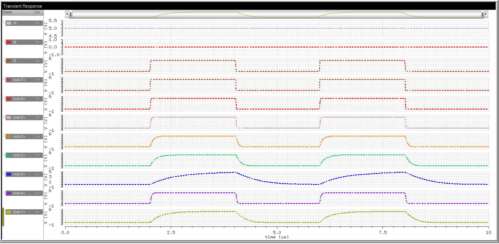
To simulate the adder, the inputs A=11001011 and B=10001001. Shown below is the schematic and results,
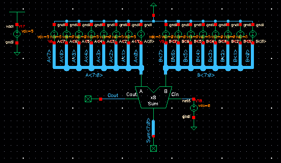
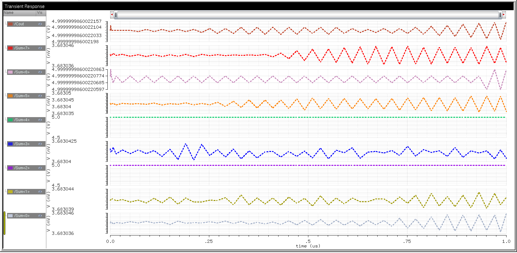
Ignoring
the oscillation on the outputs (it's a very minor oscillation anyway),
the output is out=A+B=11001011+10001001=1 01010100.
Lastly,
the 8-bit adder was created in layout. Shown below is an individual
cell of the adder, as well as all of the adders together in the layout,
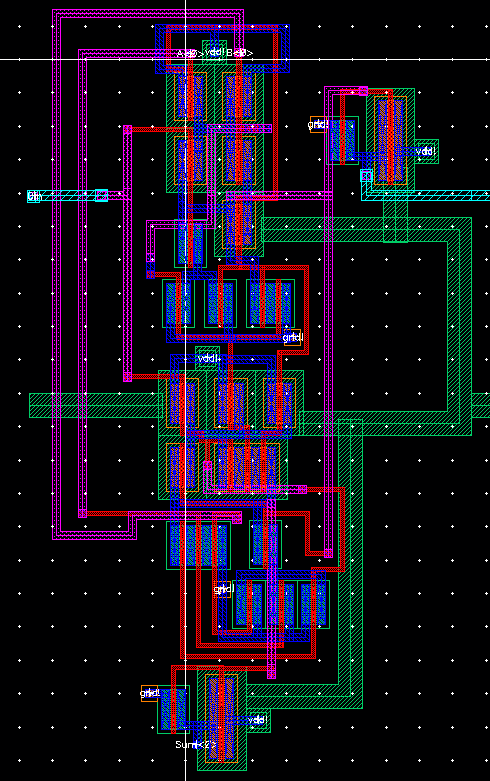

This layout DRC'd and LVS'd correctly,

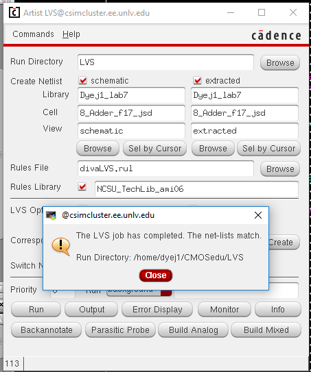
All of the files associated with this lab have been backed up in Google Drive.
Return to EE 421L Labs