Lab 6 - ECE 421L
Authored
by John Dye (dyej1@unlv.nevada.edu),
October 25, 2017
Lab
description:
In this lab, we build a NAND gate and an XOR gate, then used those two gates to develop a full adder.
Prelab:
All previous coursework has been backed-up.
Lab Report:
To
create the layouts in this lab, I needed to first create a standard
cell frame that could be instantiated into the layouts created in this
lab. The resultant standard cell frame is shown below,
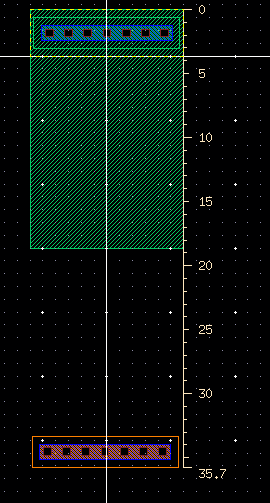
The height of the standard cell became 35.7um after trial and error
with getting the cell big enough to fit all of the required components
on the layout.
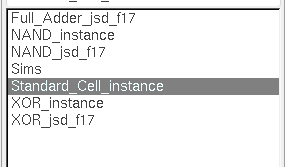
Ignoring the cells made
to be used to instantiate, the names used in the design match the
criteria for naming specified in the write-up,
To
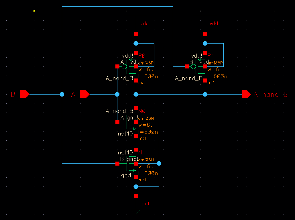
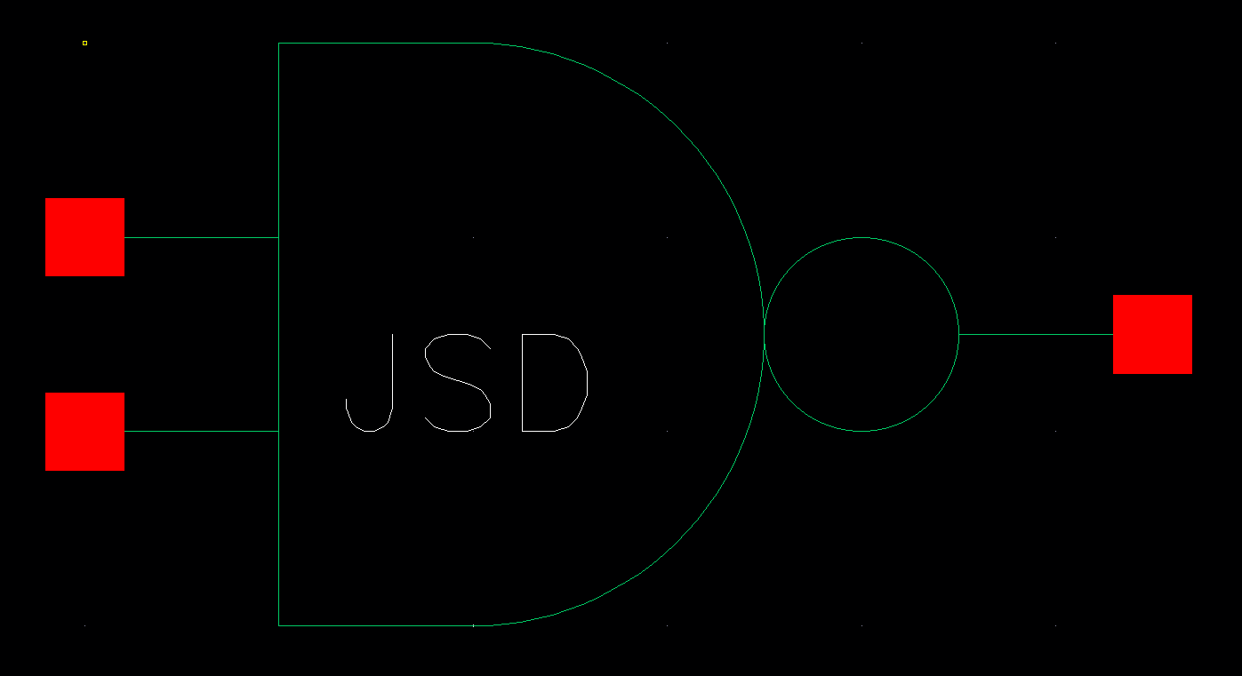
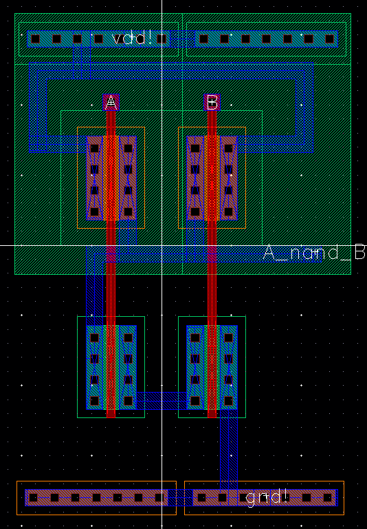
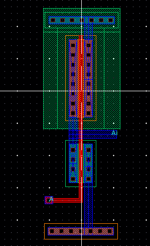
begin, a NAND gate was build as instructed in the lab write-up. Below
are the schematic, symbol, layout, DRC result, and LVS result for the
designed NAND gate,


The simulations of the schematic are included at the very end of this
report, where everything was simulated all at once.
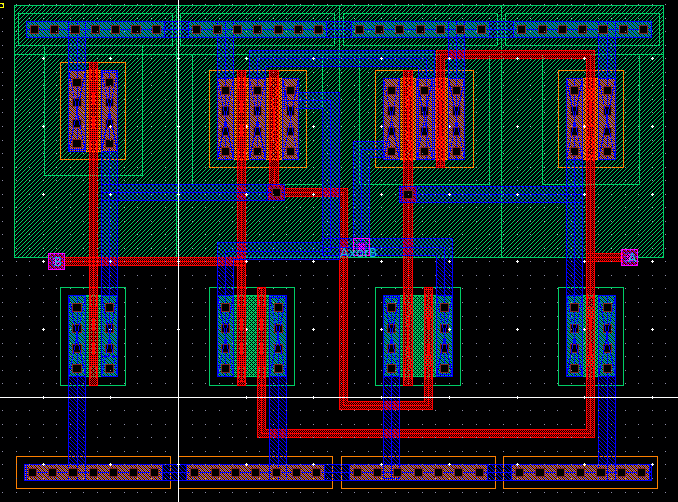
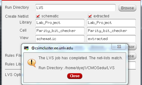
Shown below is the schematic, symbol, layout, DRC result, and LVS result for the XOR gate,
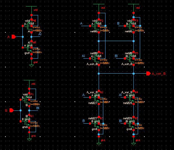
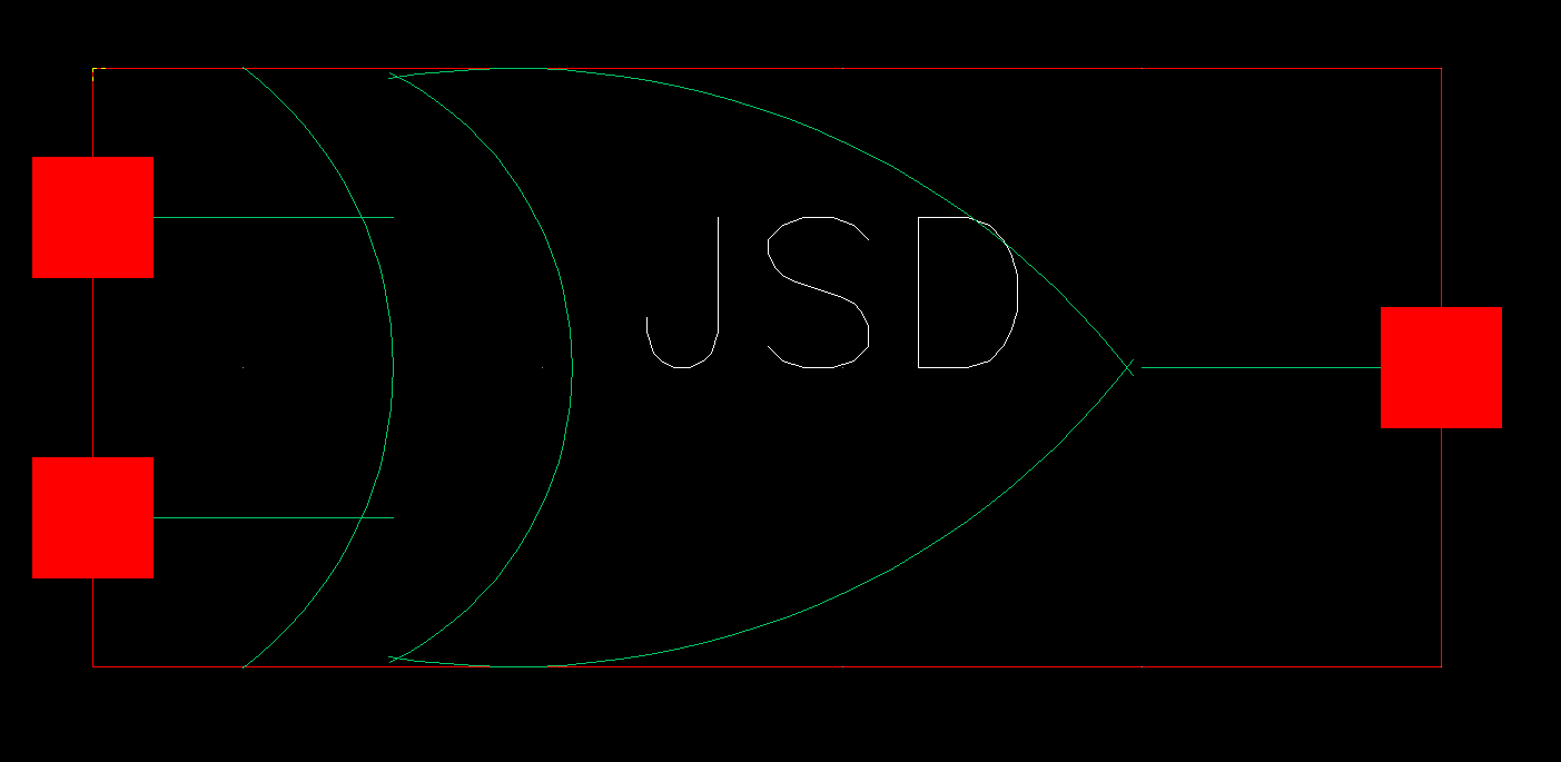
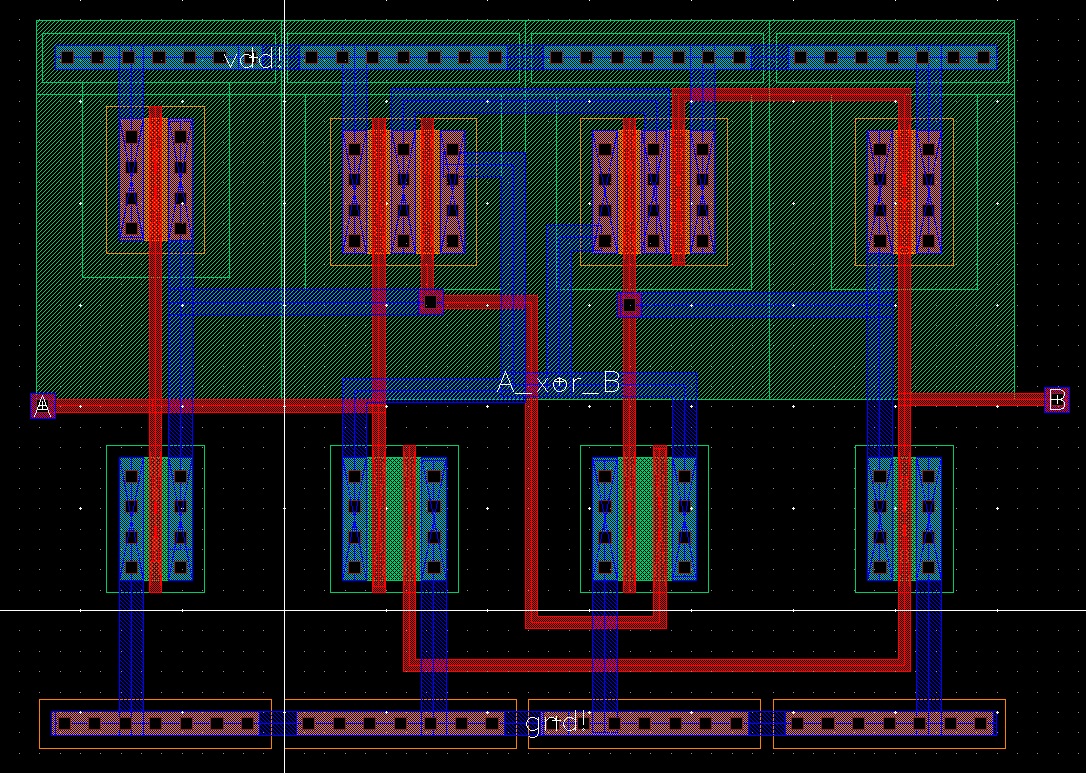


Once again, the XOR simulation are shown at the very end of this document.
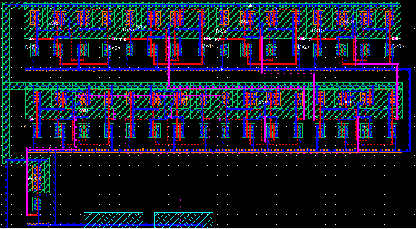
Next, a full adder was designed using the aforementioned XOR and NAND
gates. Below is shown the schematic, symbol, layout, DRC results, and
LVS results for the full adder,

Lastly, all of the created components were simulated simultaneously.
The inputs were arranged by the three voltage sources having varying
periods, resulting in the 000, 001, 010, etc. combinations,


Which shows the correct and expected results for all of the logic gates.
When the inputs are initally set, the output goes through a state of
adjusting between its initial and final values. Not only does this
transition require time to perform, but other issues such as
metastability can occur. Therefore, a certain amount of time needs to
be waited after applying inputs before the output can be fully trusted.
All of the files associated with this lab have been backed up in Google Drive.
Return to EE 421L Labs