Lab 5 - ECE 421L
Authored
by John Dye (dyej1@unlv.nevada.edu),
October 11, 2017
Lab
description:
In this lab, we used a PMOS and an NMOS to create an inverter.
Prelab:
All previous coursework has been backed-up.
Lab Report:
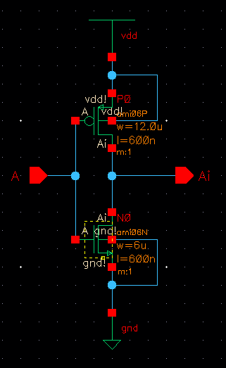
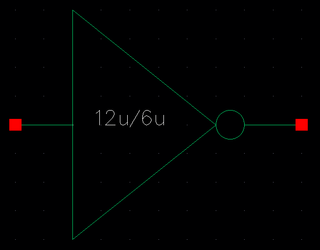
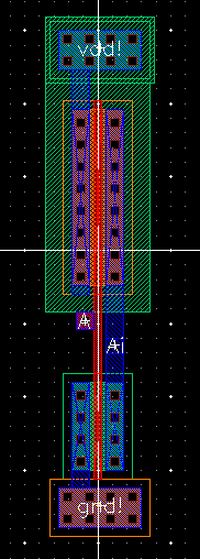
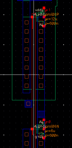
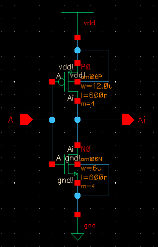
Shown below are the schematic, symbol, layout, extracted view, DRC result, and LVS result for the 12u/6u inverter,


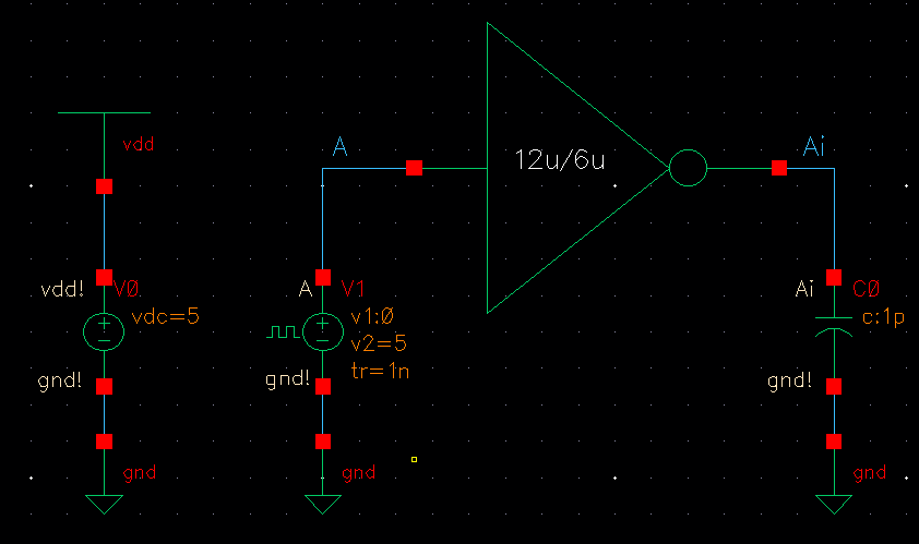
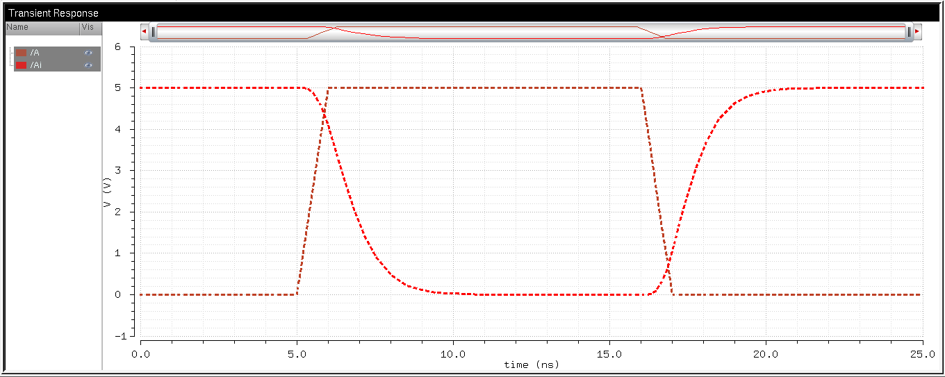
Simulating the above symbol in the schematic shown below results in the following transient response,
Then,
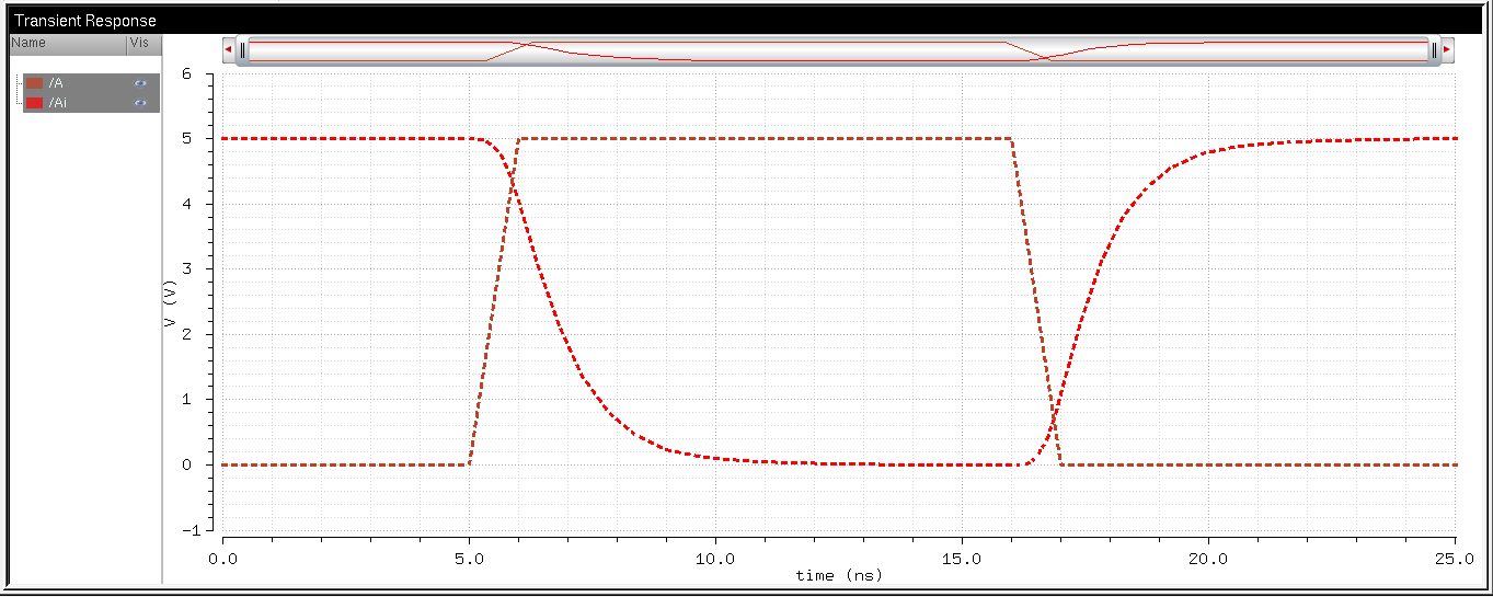
switching the simulator from spectre to UltraSim and adding the global
assignments results in virtually the same transient response,
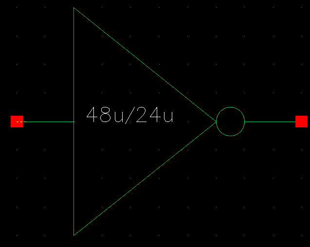
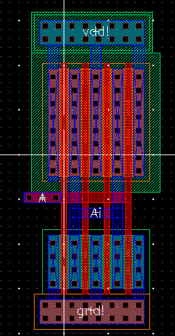
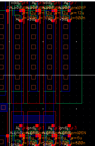
Shown below are the schematic, symbol, layout, extracted view, DRC result, and LVS result for the 48u/24u inverter,


Simulating the above symbol in the schematic shown below results in the following transient response,
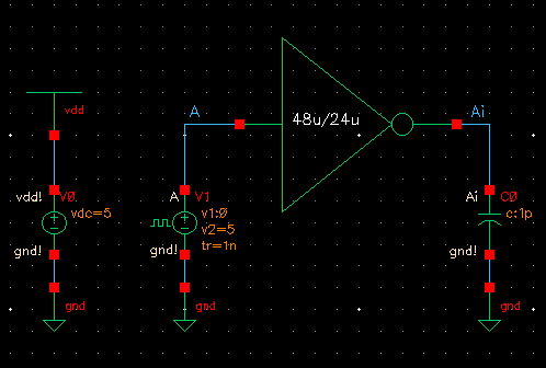
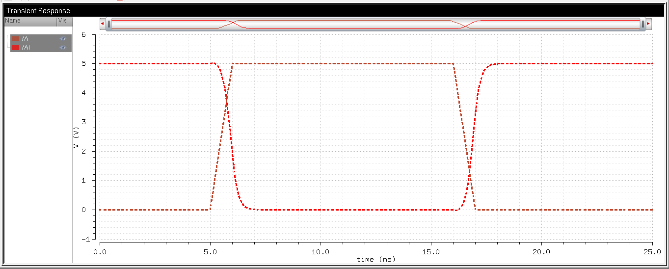
Then,
switching the simulator from spectre to UltraSim and adding the global
assignments results in virtually the same transient response,

All of the files associated with this lab have been backed up in Google Drive.
Return to EE 421L Labs