Lab 4 - ECE 421L
Authored
by John Dye (dyej1@unlv.nevada.edu),
September 27th, 2017
Lab
description:
In
this lab, we build and simulate PMOS and NMOS transistors with
differing voltage values in order to express an understanding of how
the transistors are made on an IC.
Prelab:
All previous work has been backed up in Google Drive.
Lab Report:
IDvVDS of NMOS:
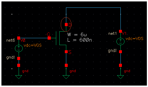
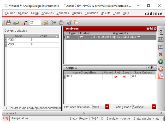
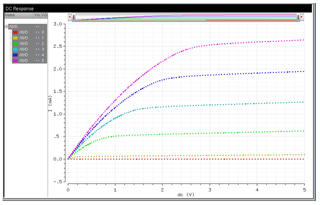
Shown
below are the schematic, simulation settings, and simulation results.
Although it is not shown here, the parameter tool was used on VGS in
order to generate these graphs,
IDvVGS of NMOS:
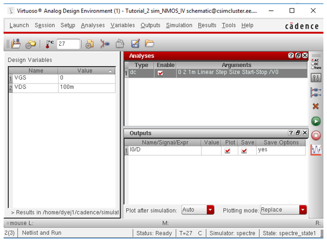
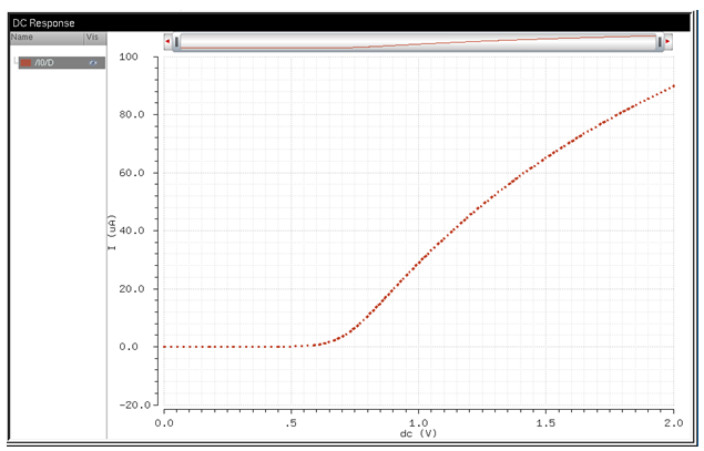
Similar
to the figures shown above, shown below are the schematic, settings,
and resultant simulation. The parameter tool was not used for this
section,

IDvVSD of PMOS:
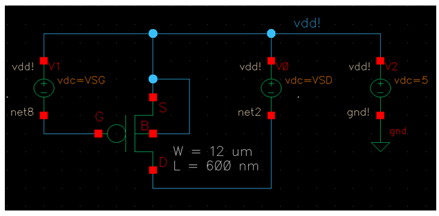
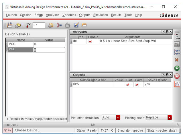
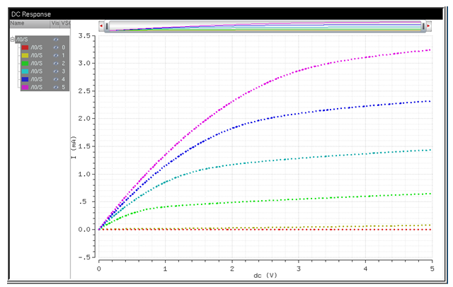
Shown
below are the schematic, settings, and result. Although not shown, the
parameter tool was used in order to generate the graph,
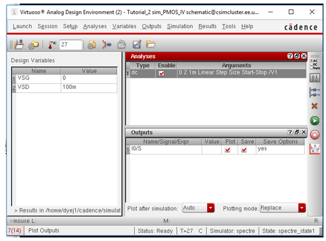
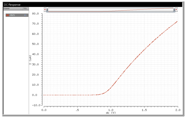
 IDvVSG of PMOS:
Below are the schematic, settings, and result. The parameter tool was not used,

6u/0.6u NMOS:
To
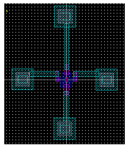
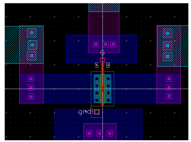
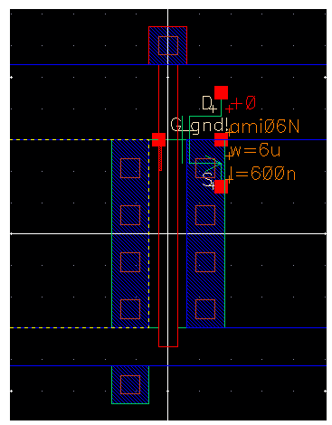
start out with, I designed the layout of an NMOS device connected to
four of the probe pads, which resulted in the following full and zoomed
in views,
Which DRC'd correctly, as shown below,

Which was then extracted to result in,
Next,
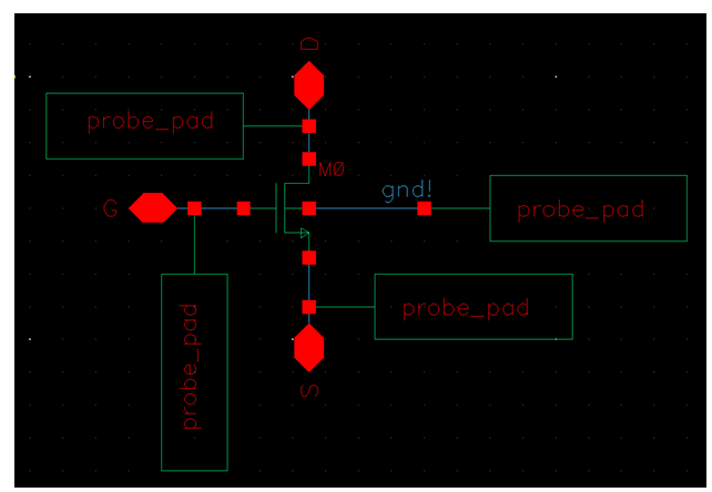
the schematic corresponding to the above layout was built. The figure
on the left is the made schematic, and the figure on the right shows
the schematic for the "probe_pad" cell,

All of which LVS'd correctly,

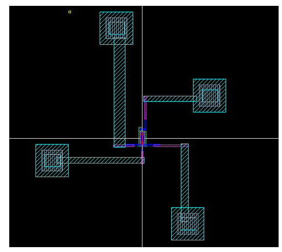
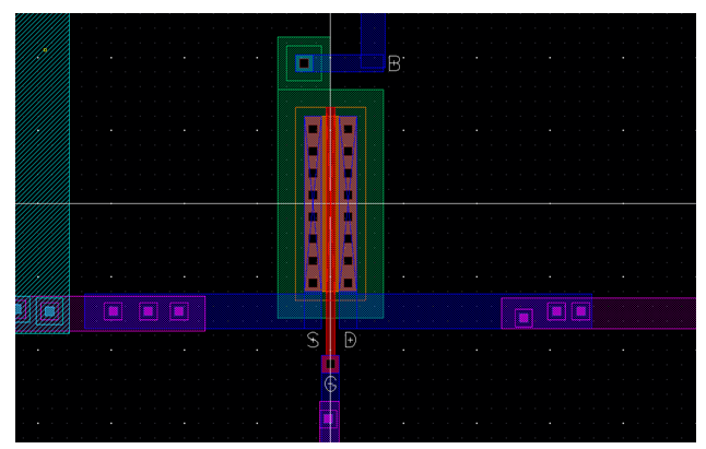
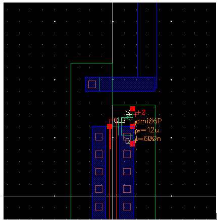
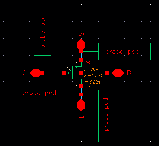
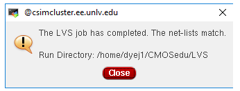
12u/0.6u PMOS:Shown below are the layout, DRC result, extracted view, schematic, and LVS report for the PMOS,


All of the files associated with this lab have been backed up in Google Drive.
Return to EE 421L Labs