Lab 2 - ECE 421L
Authored
by John Dye (dyej1@unlv.nevada.edu),
September 13th, 2017
Lab
description:
The
purpose of this lab is to go over the design as well as the
functionality of a DAC component. We start by designing the DAC system
in Cadence Virtuoso, then performing some specified simulations in
order to view the changes caused to the system.Prelab:
Narrative of the steps:
Note:
I am rather unsure about what this section is asking for, so I am going
to simply paraphrase the steps listed in the lab write up.
Start out by downloading the file linked in the lab write-up. After
uploading that file into MobaXterm, input the "unzip" command into the
command window. Even though these files have been added to the file
directory, they will not yet be able to be accessed through the library
manager. To add the file to the library manager, open the cds.lib file
in the CMOSedu folder and add a "DEFINE" command at the bottom of the
page, including the name of the library as well as the file directory.
Now, open the sim_ideal_ADC_DAC file, then simulate.
Discussing the results:
When running through the ADC, the inputted sine wave is broken down
into a binary number showing the input's relationship to the reference
voltage - the most significant bit represents 1/2 the reference
voltage, the next bit represents 1/4 the reference voltage, etc.
That signal is then
run through the DAC, which converts the binary representation of the
inputted signal back into its analog representation. This
is accomplished by running the digital signal through many different
voltage
dividers, each stage of which halves the reference signal, causing the
outputted signal to be the the summation of all of the individual
fractions of the reference signal.
This process is simulated below,
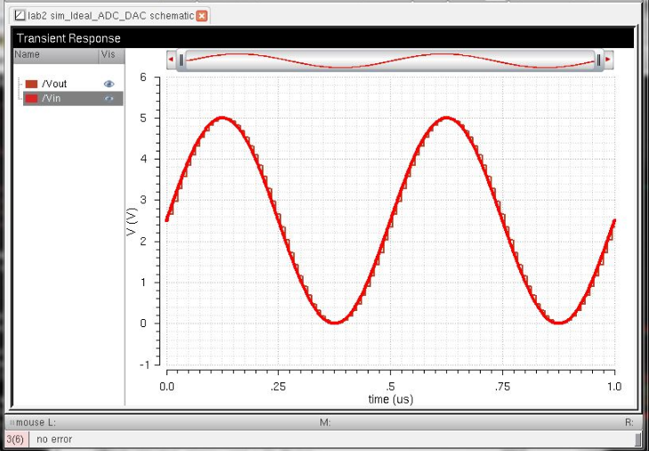
As can be seen, the input and output look nearly equivalent, except
that the output has a sort of "staircase" nature to it. This is because
of the clock. The DAC and ADC are not continuously sampling signals,
but are instead only taking a sample of the signal once every clock
cycle, causing that staircased output.
Determining the least significant bit:
Lab Report:
To start out with, I designed a DAC in cadence, shown below,
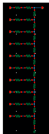
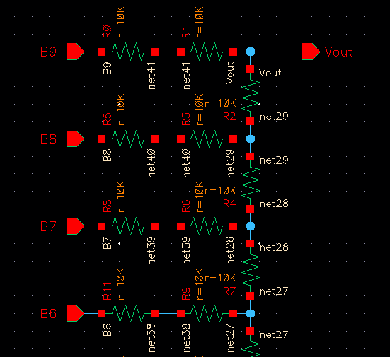
To
determine the DAC resistance, begin at the bottom node and create a
thevenin equivalent circuit. After thevenizing, combine series and
parallel resistors, then thevenize the next node. Continue up the
ladder until everything has been combined, resulting in the equivalent
resistance being R.
Example: R_thevenin
= (R_1+R_2) || R_3. This result is then in series with the next
vertical resistor, then keep thevenizing.
0.7RC = 0.7(10k)(10p)=70ns
According to the sim,
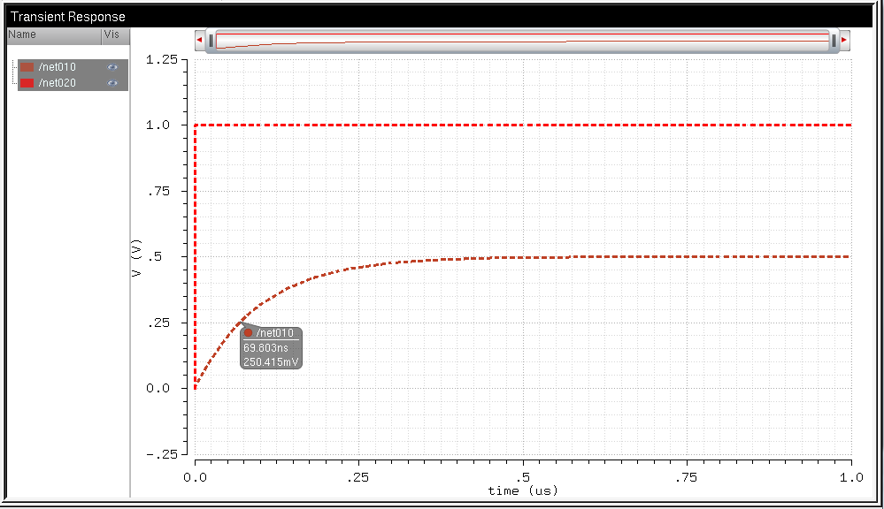
Which matches the calculated result of 70ns.
To
create a new symbol, we will be using a premade symbol, deleting the
contents of that symbol and removing any unnecessary pins, then copying
our schematic into it, which results in the symbol,
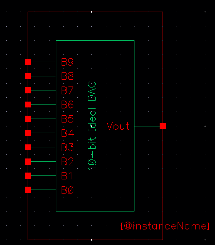
Which is then inserted into the ADC DAC sim file, resulting in,
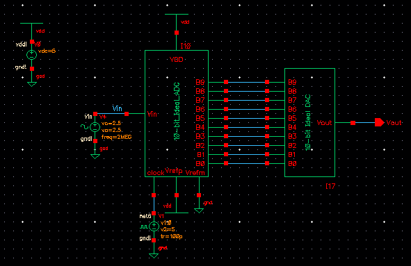
Which simulates as,
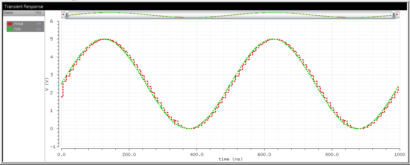
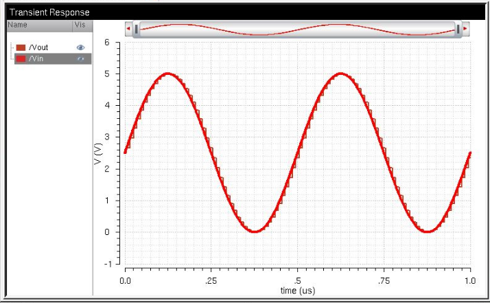
The resultant sim is on the left and the original
sim is on the right. As can be seen, they are nearly equivalent.
Applying a 10k resistor results in the following model and simulation,
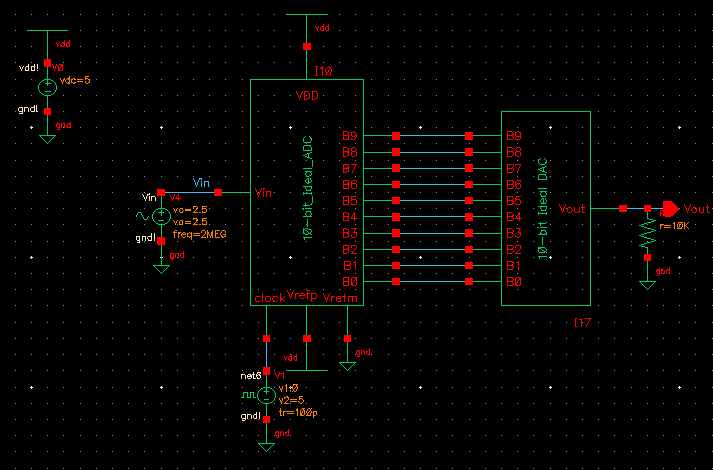
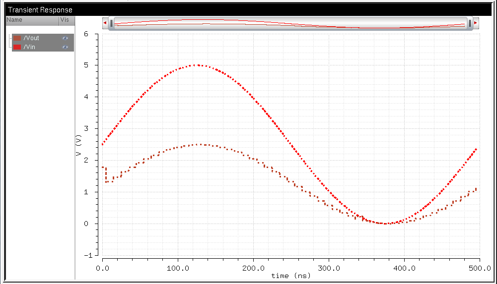
The output ended up being halved because the output
resistance doubled - went from R to R+R=2R, cutting the voltage in half.
Applying a capacitor value of 10pF,
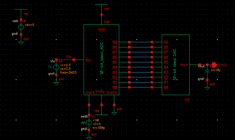
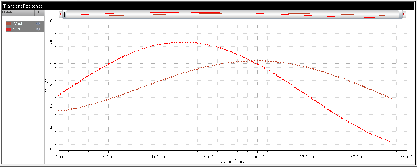
A visible delay can be seen.
Applying both a 10k resistor and a 10pF capacitor results in,
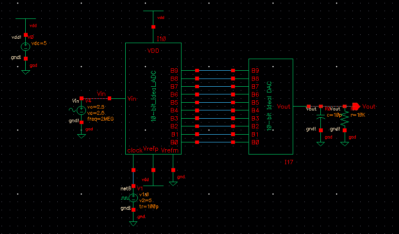
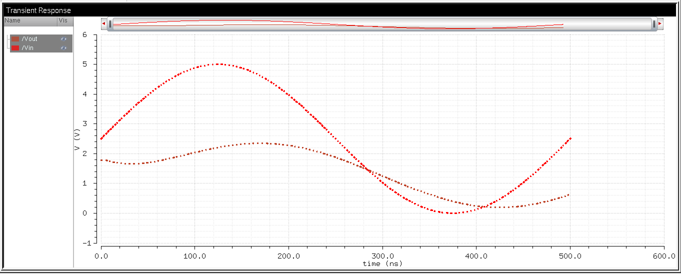
Which shows both the delay and the voltage drop.
If
the resistance of the switches isn't small comparable to R, then when
the switches are open they won't act like switches, they will instead
act like resistors. This will cause a substantial voltage drop in
betweenthe input and output while the switch is open, meaning voltage will still be allowed through to corrupt our results.
This lab and its associated materials have been backed up in google drive.
Return to EE 421L Labs