Lab 3 - EE 421L
Jeeno Doria
doriaj3@unlv.nevada.edu
9/12/2017
Lab
description: Create a layout of the previous 10-bet DAC in lab 2.
Pre-lab work
- Back-up all of your previous work from the lab and the course.


Lab: In
this lab parts in Tutorial 1 and lab 2 used. We are to create a
layout of a 10-bit DAC and simulate its extracted verison.
- Discuss,
in your lab report, how to select the width and length of the resistor
by referencing the process information from MOSIS

-In
MOSIS, the sheet resistance is 800ohms/square. If we want to achieve a
particular resistance, we can use the following steps below if we
wanted 10.26K.
The width of the n-tap with two rows is 4.5microns.
In the layout window pick the n-well layer=> R key=> Enter key. R
will create shape the n-well as a square, or rectangle to your desired
sizing. When you hit Q on the n-well, a small window seen above will
pop up. These will show the specs of the n-well. Left, Right, Bottom,
and Top are just positions in the layout, but the actual size of the
n-well is in the Height and Width box.


After you get the n-well sized to your choosing, select the res-id metal and size it perfectly right over the n-well. To check for errors, go to the Verify tab=>hit DRC.

- Discuss, in your lab report, how the width and length of the resistor are measured
-The ruler tool can measure the length and width. To use the ruler, hit K and pick two points.

After
you have checked for no errors, hit the Verify tab once more then
select Extract. Go back to the library manager and the particular cell
view that had the layout. The cell view will now have an extracted file
listed. The image above is an example of an extracted layout.
The next step was to create a DAC layout.
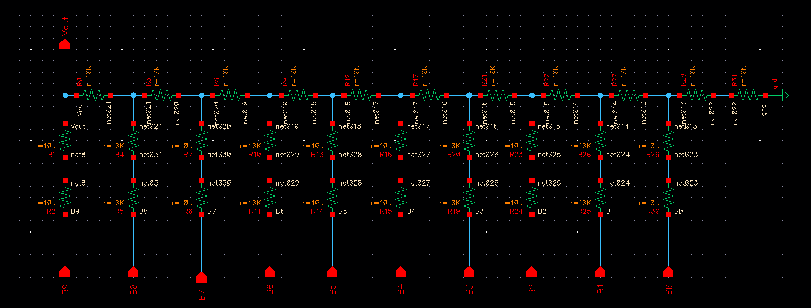
DAC schematic:

- Ensure
that each resistor in the DAC is laid out in parallel having the same
x-position but varying y-positions (the resistors are stacked)
- All input and output Pins should be on metal 1
DAC layout:

After this layout was finished, DRC the layout to check for errors and create an extracted version.

Extracted file:

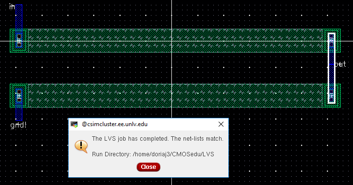
- DRC and LVS, with the extracted layout, your design (show the results in your lab report)
Hit the verify tab => LVS, which stands for Layout VS schematic. I am comparing the DAC schematic from lab 2 with the layout.

After hitting run and it had completed comparing the two files, hit output to double check that it had really matched.

Finally
we have to simulate and compare the wave forms. In order to simulate
the extracted layout, we have to hit the ADE L window of the schamtic
we want and hit setup => environment. A window like this will pop up, but infront of where it says schematic we must add extracted.

After that we go to the simulations tab => netlist => display. We get the following window below.

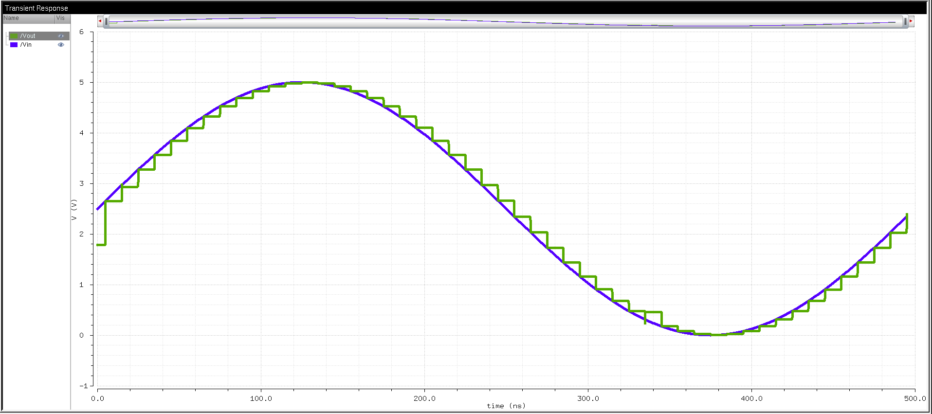
Comparing simulations:
No load => R Load => C Load => RC Load
| Schematic Simulation | Extracted Simulation |
 |  |
 |  |
 |  |
 |  |
Cadence Files: attachment.zip
Return to my labs