EE 421L
Lab 8
Authored
by Jeremy Morgan, Preston Donovan, Miguel Morga
Email: morgaj7@unlv.nevada.edu, donovp@unlv.nevada.edu, morga@unlv.nevada.edu
Due: 12/6/2017
Lab Description:
Generation of Test Chip
LAB 8 DIRECTORY (zip file): HERE
Overall:
Chip Contents:
2 - Course Projects (Jeremy, Preston)
1 - 31 stage ring oscillator (w/buffer)
1 - 6/.6 NMOS
1- 12/.6 PMOS
1 - NAND Gate (6/.6 NMOS - 12/.6 PMOS)
1 - NOR Gate (6/.6 NMOS - 12/.6 PMOS)
1 - XOR Gate (6/.6 NMOS - 12/.6 PMOS)
1 - Inverter (6/.6 NMOS - 12/.6 PMOS)
1 - 25k Resistor
1 - 25k / 10k Voltage Divider
1 - 100k High Res
1 - 50k High Res
1 - Bandgap
1 - XNOR Gate (6/.6 NMOS - 12/.6 PMOS)
Pin Connections:

Using Chip
Insert Chip into breadboard.
Ground is global at pin <20>. Make sure to ground. VDD is not global.
Use pin diagram above and chip diagram below to test various functions of chip (highlighted above).
Example (testing Inverter):
Ground gnd! at pin <20>
Insert VDD into pin <35>
Insert a voltage into pin <34>
Ai at pin <36> should now be inverse of pin <34>
Chip Diagram (pin locations)


Chip Design:
Schematic:

Layout:

LVS:

DRC:

Components of Chip:
31-Stage Ring Oscillator:
Schematic
Symbol


NAND:
Schematic
Symbol


NOR:
Schematic
Symbol


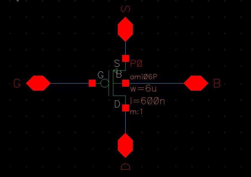
PMOS:
Schematic
Symbol

NMOS:
Schematic
Symbol


Voltage Divider (25k / 10k):
Schematic
Symbol


Inverter:
Schematic
Symbol


Bandgap:
Schematic
Symbol


XOR:
Schematic
Symbol


XNOR:
Schematic
Symbol


Course Project (Preston):
Schematic
Symbol


Course Project (Jeremy):
Schematic
Symbol


LAB 8 DIRECTORY (zip file): HERE
Return to EE 421L Labs