
Lab 7 - ECE 421L
Postlab:
I created a symbol and schematic for a 4 bit inverter. By using busses I can easily compact my circuit; rather than creating 4 different circuits I can simplify them into one.
Schematic:

Simulation:

Results:
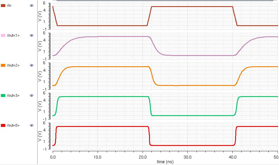
The output shows it is running 4 seperate inverters wiht different capacitence loads, which is what I expected.
I repeated this process but instead made it 8 bits and did it for an inverter, and for AND, OR, NAND, and NOR gates.
| Gates | Schematic | Symbol | Simulation | Output |
| Inverter |  |  |  |  |
| AND |  |  |  |  |
| OR |  |  |  |  |
| NAND |  |  |  |  |
| NOR |  |  |  |  |
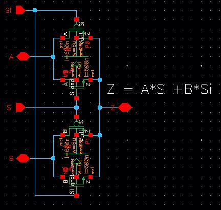
Next I created a 2-to-1 DEMUX/MUX. I used this schematic and symbol.

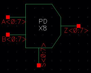
And made it 8 bit as well as took out the Si input by adding an inverter. Here are the 8 bit schematic and symbol

I then tested the multiplexing.

And got this as an output:

The multiplexer works by selecting A when input S is high and selecting B with input S is low and passing the signal of the selected input.
Next I tested the Demultiplexing.

And got this as an output:

Demultiplexing is doing the opossite of multiplexing, meaning when S is high A=Z and when S i slow B=Z.


And made this symbol:

To make it 8 bit I again used busses.

I didn't want to connect the last cout into the first cin to avoid overflow.
Then created a new symbol for an 8 bit adder:

When I simulated it I got what I expected. It worked like the full added in the last lab.


Finally I created a layout for the full adder. I started with one and thought ahead so I could easily chain the next ones together, becasue I couldnt use busses in the layout.

When I connected 8 of these side by side, I also had to rename each An, pin to An<0>, An<1>... An<7> in order and I did the same for the Sn and Bn pins. The Cn pin is only read on the first adder, and the cout (Cn+1) is fed into the next adder on its own.

I then DRCed and LVSed my layout and they passed!

