Lab 6 - ECE 421L
Authored
by Preston Donovan,
donovp1@unlv.nevada.edu
October 24 , 2017
Prelab:
Backup previous labs
Do Tutorial 4
Postlab:
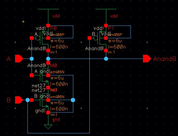
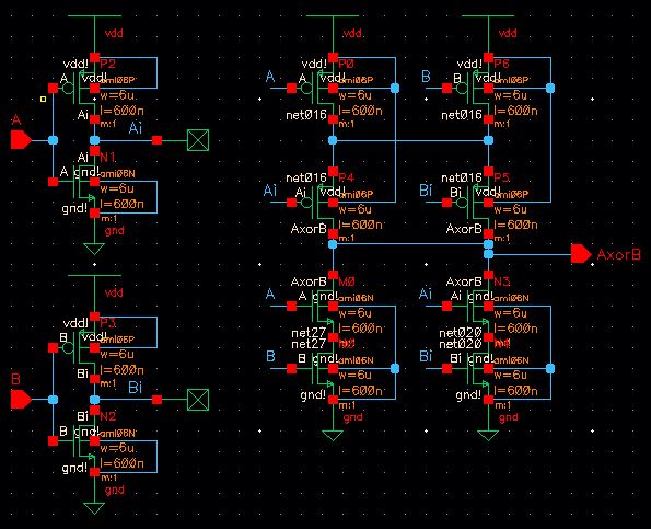
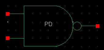
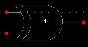
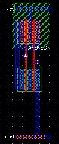
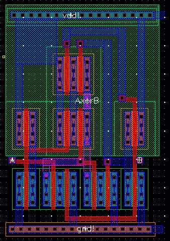
I created schematics, symbols, and layouts for a 2-input NAND and XOR gate using 6u/0.6u MOSFETs.
Note
that I made each layout the same height and they will automatically
connect gnd! and vdd! when each layout is directly placed next to
eachother.
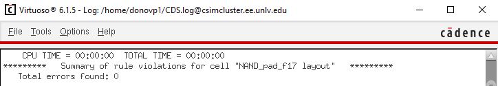
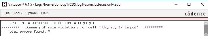
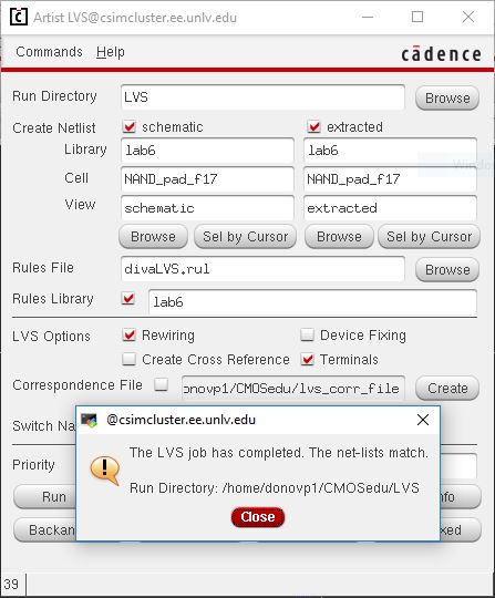
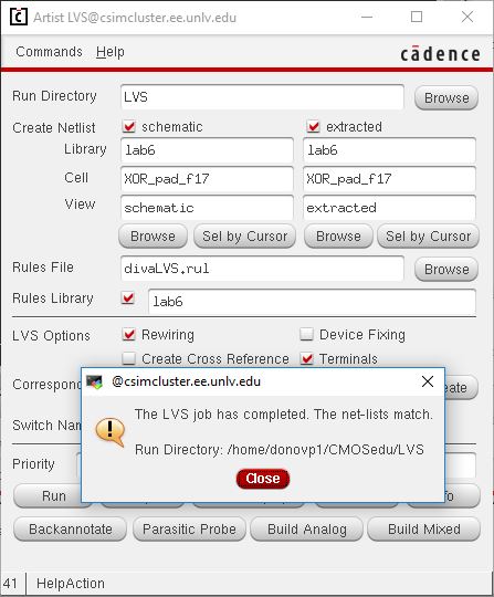
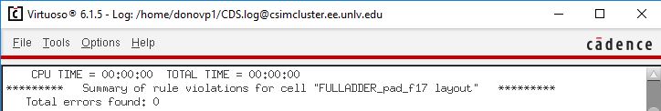
Both layouts DRC and LVS.
Then I simulated these gates to see how they work.
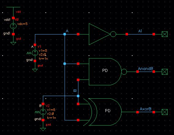
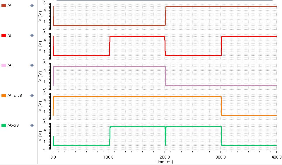
The
results are what I expected but there is a glitch in the XOR. It looks
like it happens because the rise and fall time for the inputs are not
instantaneous. If they were quicker, the glitch would be smaller.
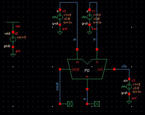
Next I created a Full-Adder schematic, layout, and symbol.
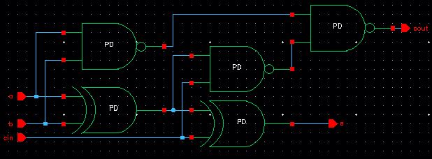
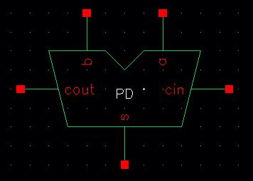
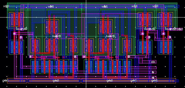
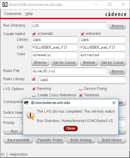
The layout also passes DRC and LVS.
Lastly I simulated the Full Adder to see if I got the expected results of
a | b | cin | | s | cout |
0 | 0 | 0 | | 0 | 0 |
0 | 0 | 1 | | 1 | 0 |
0 | 1 | 0 | | 1 | 0 |
0 | 1 | 1 | | 0 | 1 |
1 | 0 | 0 | | 1 | 0 |
1 | 0 | 1 | | 0 | 1 |
1 | 1 | 0 | | 0 | 1 |
1 | 1 | 1 | | 1 | 1 |
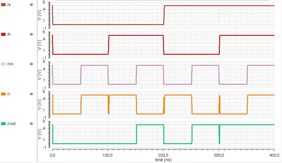
The outputs match how I expected!
Return to EE 421L Labs