Lab 4 - ECE 421L
Authored
by Preston Donovan,
donovp1@unlv.nevada.edu
September 27, 2017
Prelab:
Complete Tutorial 2
Backup all work
Postlab:
1. A schematic for simulating ID
v. VDS of an NMOS device for VGS varying from 0 to 5 V in 1 V steps
while VDS varies from 0 to 5 V in 1 mV steps. Use a 6u/600n
width-to-length ratio. 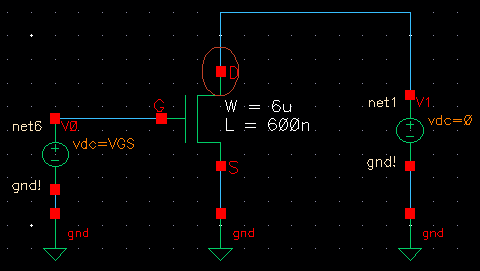
I used parametric analysis for VGS with linear steps of 1 from 0 to 5.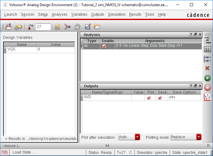
And got this as an output.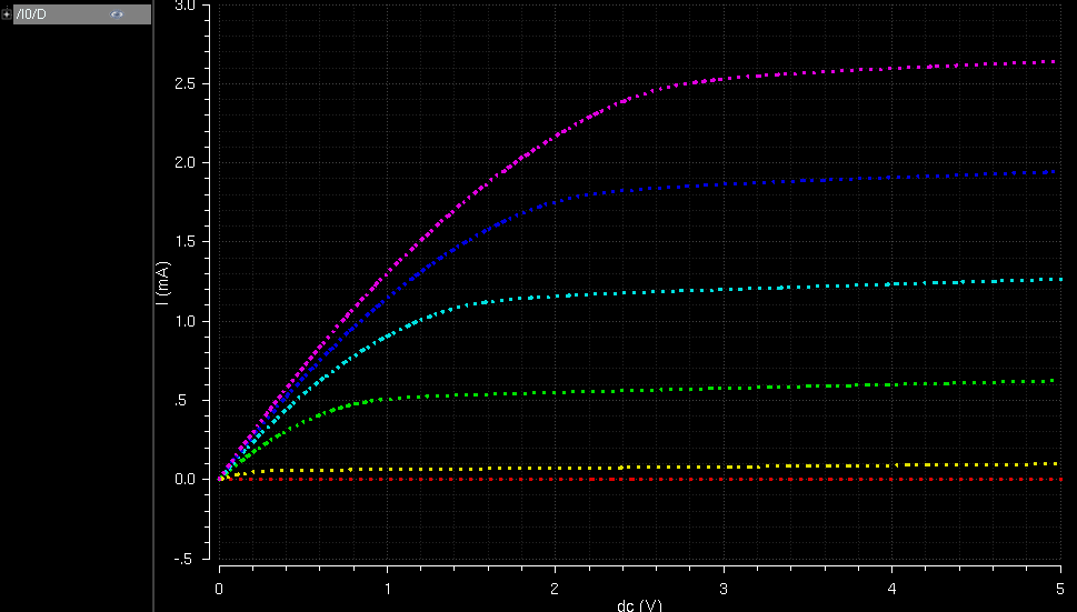
2.
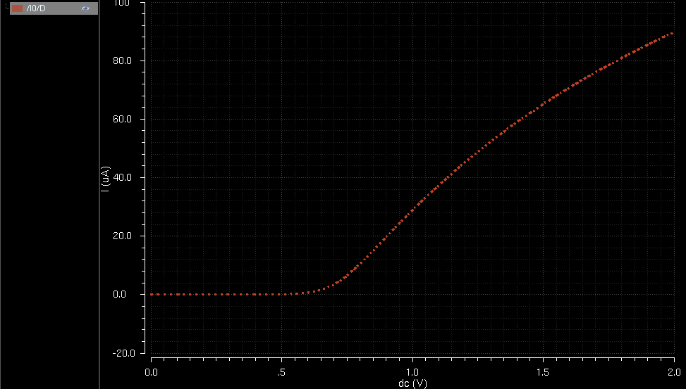
A schematic for simulating ID v. VGS of an NMOS device for VDS = 100 mV
where VGS varies from 0 to 2 V in 1 mV steps. Again use a 6u/600n
width-to-length ratio.
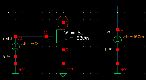
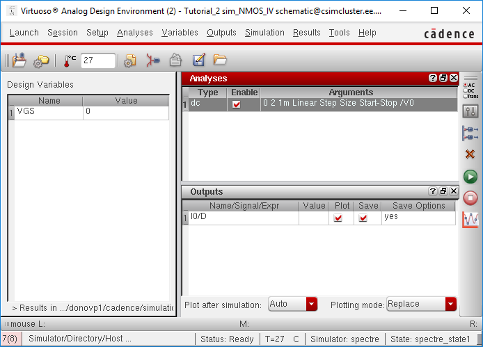
And got this as an output.
3.
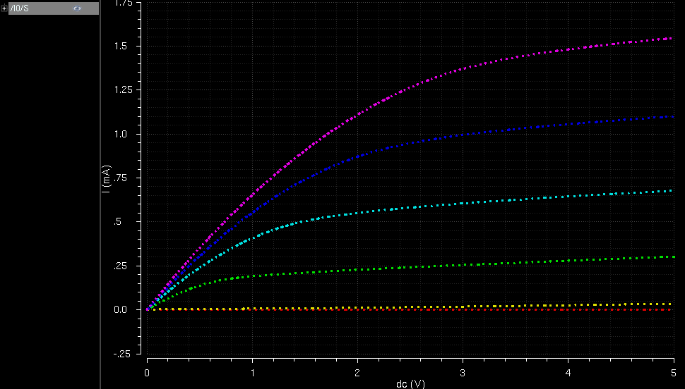
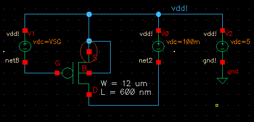
A schematic for simulating ID v. VSD (note VSD not VDS) of a PMOS
device for VSG (not VGS) varying from 0 to 5 V in 1 V steps while VSD
varies from 0 to 5 V in 1 mV steps. Use a 12u/600n width-to-length ratio. 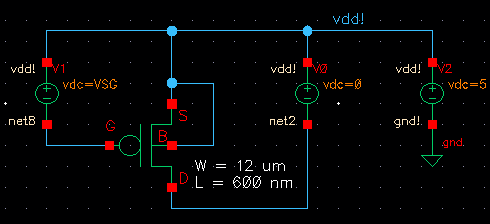
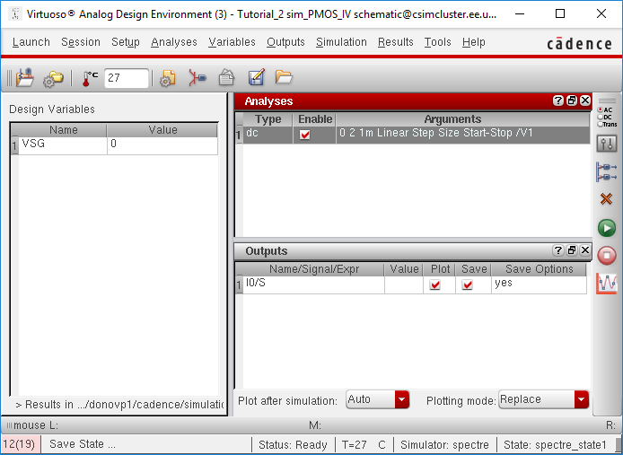
I used parametric analysis for VSG with linear steps of 1 from 0 to 5.
And got this as an output.
4.
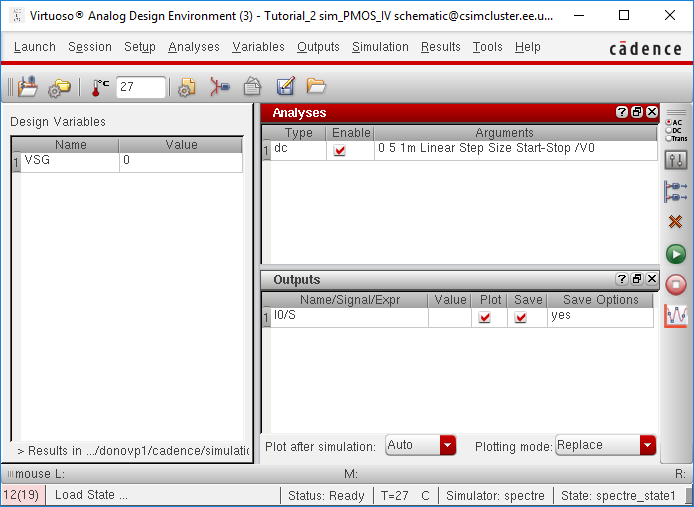
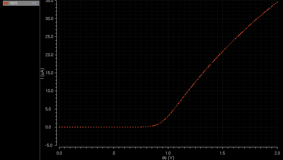
A schematic for simulating ID v. VSG of a PMOS device for VSD = 100 mV
where VSG varies from 0 to 2 V in 1 mV steps. Again, use a 12u/600n
width-to-length ratio.
And got this as an output.
Lay out a 6u/0.6u NMOS device and connect all 4 MOSFET terminals to probe pads.
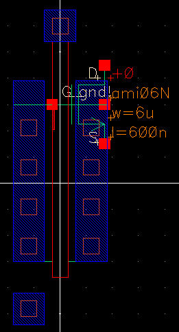
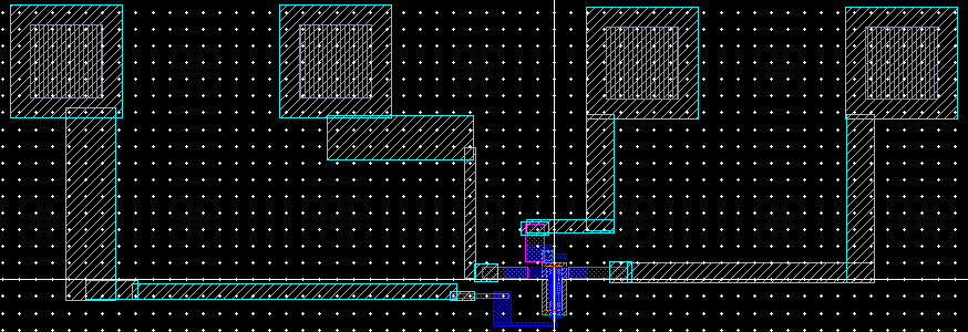
Worked my way up to metal 3.
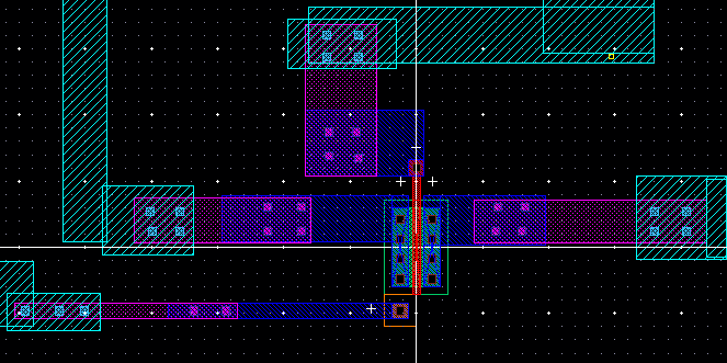
And connected it to the pads.

Then I used LVS with this schematic:
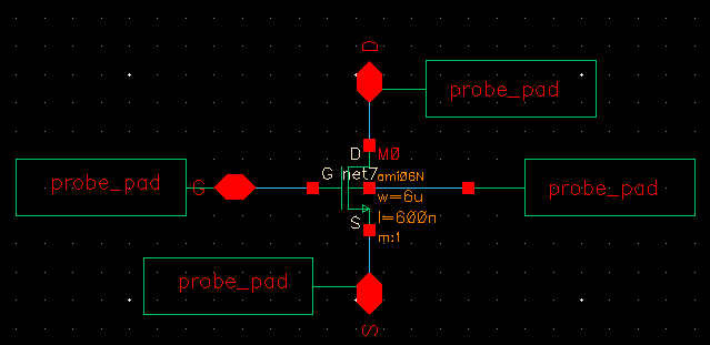
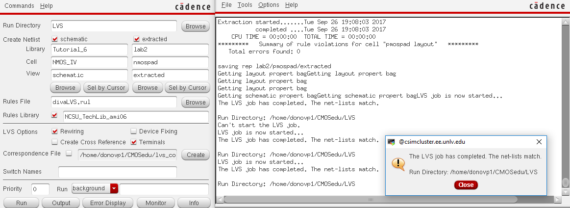
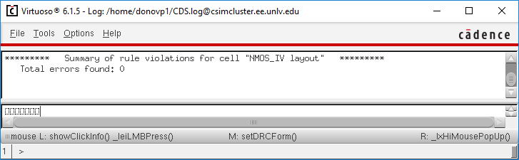
My LVS and DRC passes!
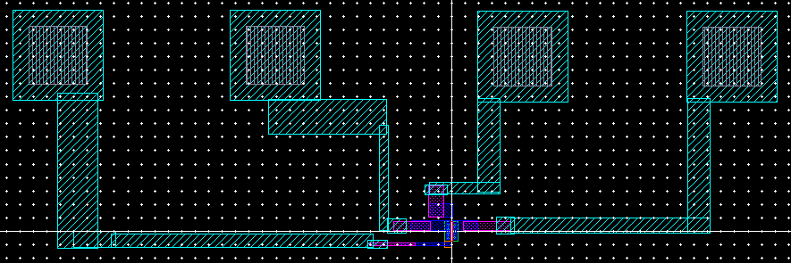
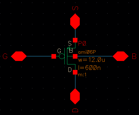
Lay out a 12u/0.6u PMOS device and connect all 4 MOSFET terminals to probe pads.
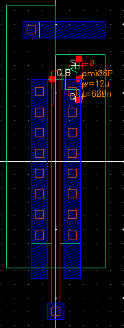
Worked my way up to metal 3.
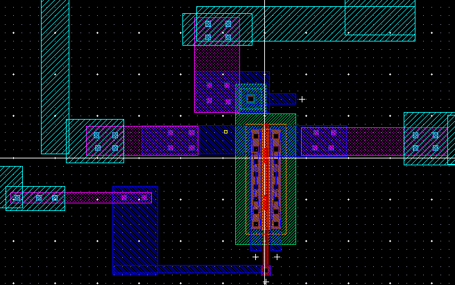
And connected it to the pads.
Then I used LVS with this schematic:
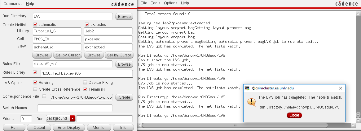 My LVS and DRC passes!
Return to EE 421L Labs