Lab 3 - ECE 421L
Authored
by Preston Donovan,
donovp1@unlv.nevada.edu
September 20, 2017
Prelab:
Complete Tutorial 1
Backup all labs
Here is a .zip file of this lab.
Postlab:
To
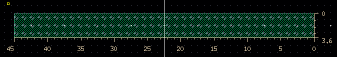
create a 10k nwell resistor I need to understand the MOSIS process
works. Using the formula R=Rsq(L/W) and given the minimum length and
width is 3.6nm and Rsq is 800 I can choose values to make nearly any
resistance. Notice that increasing W will lower my resistance and vice
versa. I want a 10k resistor, and to make it the smallest size
allowable I should choose a small W value.Let W=3.6nm, the smallest it can be.
10k=800(L/3.6nm)
Solving gives L=45nm.
Using
the ruler tool by using keybinding "k" I have displayed my nwell
dimensions that I calculated above. To clear all rulers press "Shift+k".
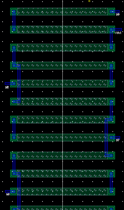
Now
I want to create an equivalent DAC to the DAC I made in lab one, but I
want all of my resistors to be stacked. Here is my design.
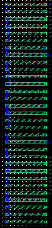
And
the full view of my layout and extracted view here. I made gnd! an
input pin. This is onething I didnt have to consider on the original
DAC.
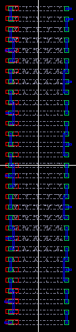
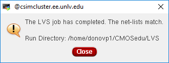
Now I will compare it to my original DAC by and LVS check.
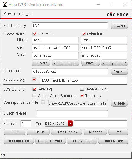
And it matched!
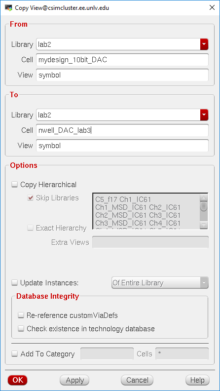
I then copied the symbol from the original DAC to my nwell DAC and renamed it. Then I replaced my old DAC with the nwell DAC.
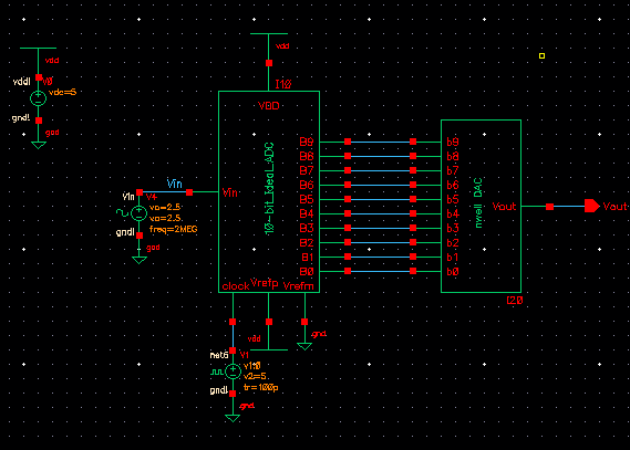
I
got an error when I simulated it. To fix it I had to make it run the
extracted view before the schematic view. To do this I went to ADEL
> Setup > Environment... and added "extracted".
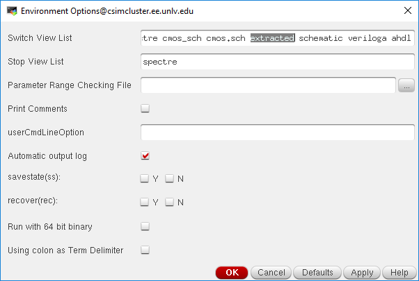
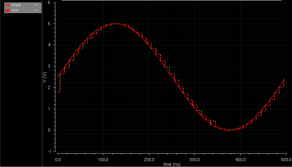
This fixed my error and allowed me to see the output with no load.
Return to EE 421L Labs