Lab 2 - ECE 421L
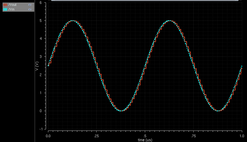
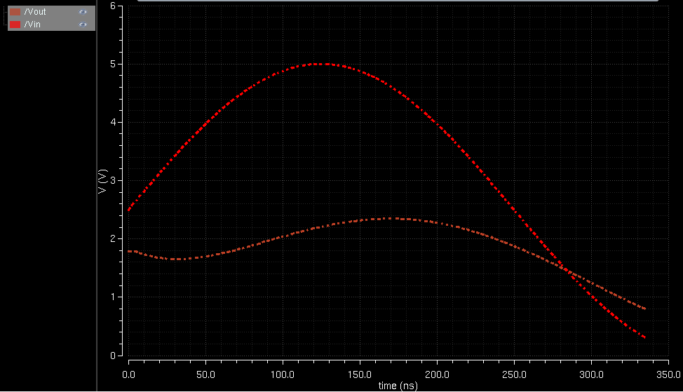
The output nearly matches the input except that it seems to be sampled from the input. The samples are spread out enough to make the output rough.
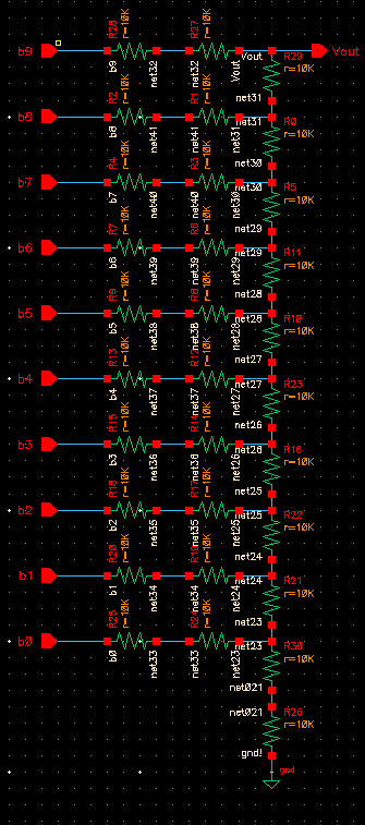
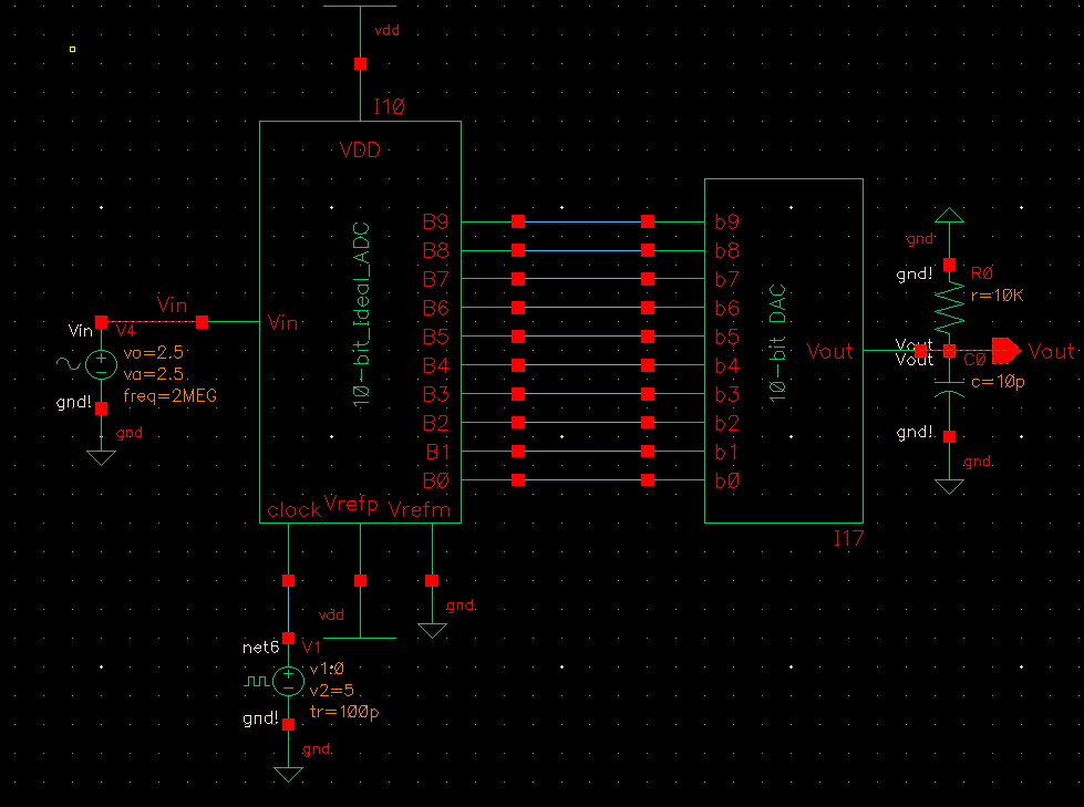
The digital code B[9:0] changes voltage value depending on the input's voltage offset. In the image above, the offset is 2.5V and each bit will have a voltage at 2.5V.
Postlab:
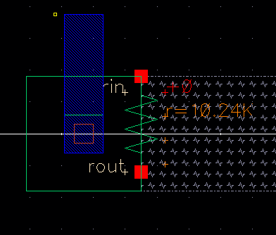
First I made an n-well resistor with 10k Ohms

I created a 10-bit DAC given figure 30.14

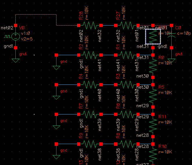
If I ground all the pins except B9 and attach a 10p capacitor load, I can calculate the time delay with the formula:
0.7RC
To determine the output resistance, notice all resistors are 10k. Starting at the bottow at B0, combine the two resistors in series infront of B0 as well as the resistors above ground. This will leave 20k ohms in parallel with 20k ohms which reduces to 10k ohms. Repeat this process up the line and by the time B9 is reached total resistance will equal 10k ohms.
R= 10k C= 10p 0.7(1000)(10*10^-12)=70n seconds.
Simulating the output gives:
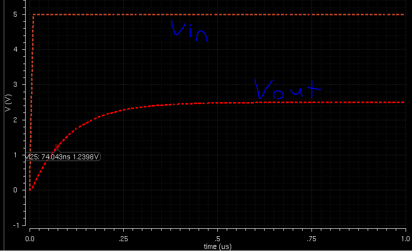

At 70ns, the output voltage is about 1/4th of the input voltage.
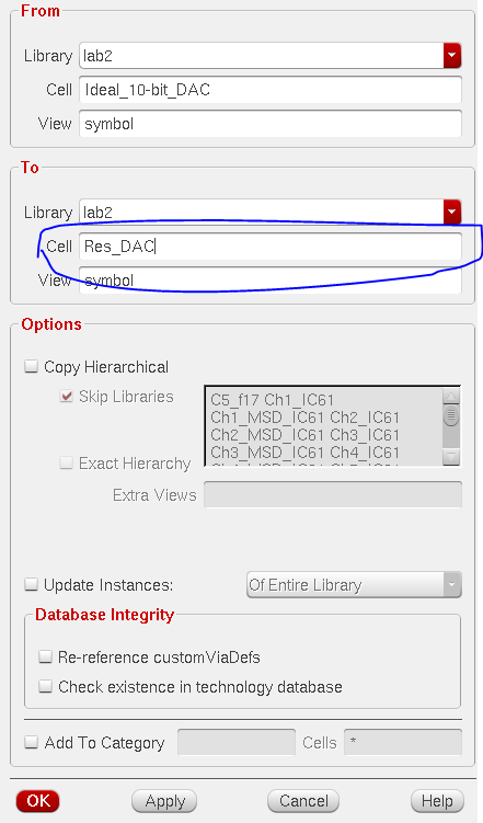
Now I want to replace the original DAC with my created DAC of resistors. I want the exact same symbol so I will copy it by going to the symbol I want and selecting copy.
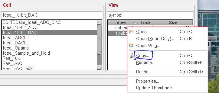

Then I will type in the name of the cell I want to copy it to and press OK. This will give me the exact symbol and I can further edit it to get rid of the unnessesary additional pins.
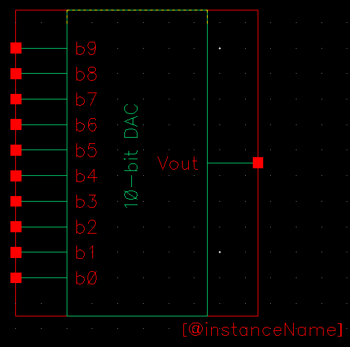
Here is my final symbol:

To test my circuit I will replace the old DAC with my new one and check the outputs when I attach three different loads of a 10k resistor, a 10p capacitor, and a 10k resistor and 10p capacitor in parrellel.
With a 10k resistor.
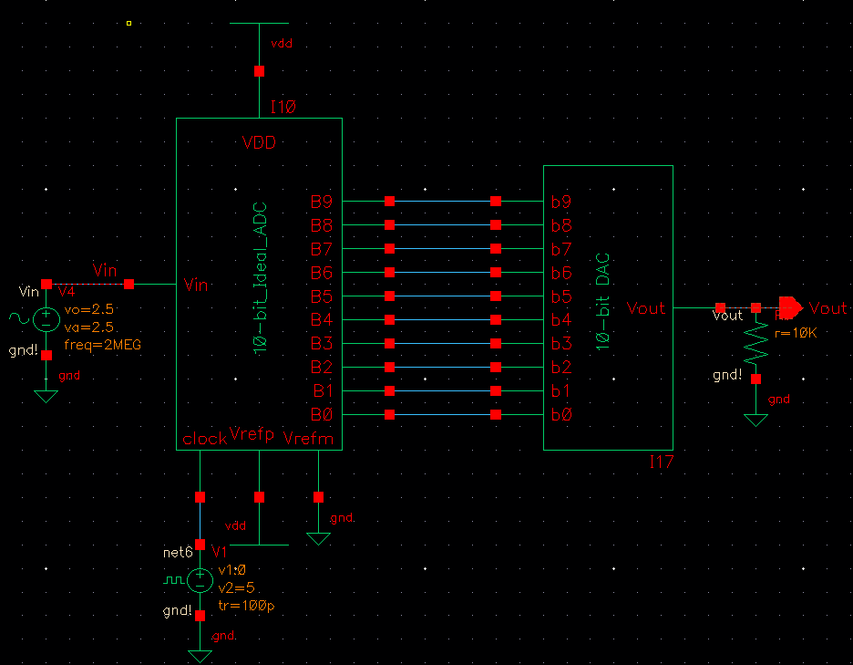

Responce to the 10k resistor load:
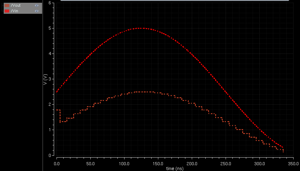

The result is half of the input. This makes sence because it created a voltage divider.
Replacing the resistor with a 10p capacitor
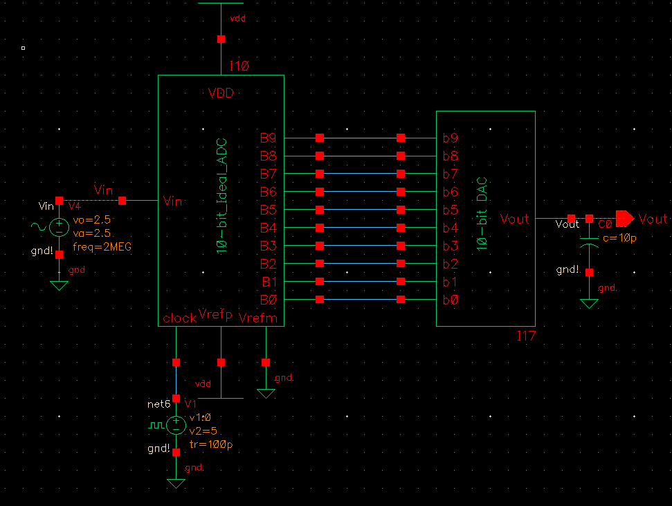

Responce to the 10p capacitor load:
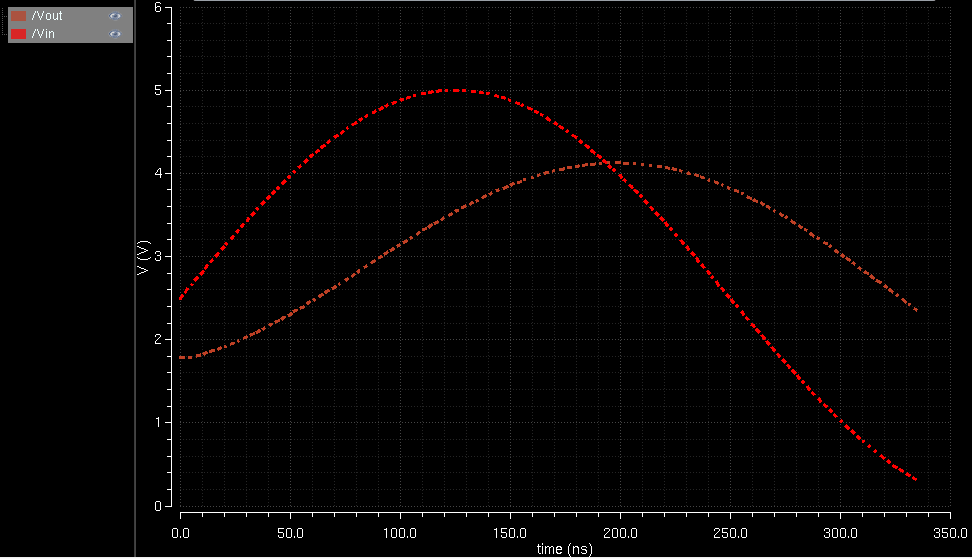

The capacitor removes the roughness of the output. Observe that the output voltage is smooth.
Adding the 10k resistor back

Responce to the 10k resistor and 10p capacitor load in parallel:

The output shows a compination of the two instances above. The voltage is halved and the output voltage is smooth.
The switches are placed between the input and 2R resistor. This will add resistance and will give different outputs. The output resistance will be much more difficult to calculate as well.
Return to Student Lab Reports