Lab Project -
EE 421L
Authored
by Reiner Dizon,
Email: dizonr1@unlv.nevada.edu
Schematic completed on November 15, 2017
Layout completed on November 22, 2017
Project description:
For this
project, the objective is to design an the even parity checking circuit
for 9-bit input word (8-bit for the data and 1-bit for the parity). It
will output a "1" if the even parity check is valid and "0" otherwise.
The main logic gates used in this project are the XOR gate and the
inverter. After designing the circuit in schematic, I laid it out and
used the tool to check its validity and its similarity with the
schematic.
PART I: SCHEMATIC
1) Design of 2-bit XOR Gate
The
2-bit XOR gate outputs "1" as long as both inputs are the different
(i.e. one input is HIGH and the other is LOW). Otherwise, the output is
"0" meaning that the inputs are the same. For that reason, I selected
this XOR gate for my parity checker because an output of "1" implies
that the inputs are of different logic level. After
checking and saving, I made the corresponding symbol of a 2-bit XOR
gate. Here are the schematic and symbol for the 2-bit XOR gate:
SCHEMATIC
 | SYMBOL

TRUTH TABLE
|
Before
using this gate for the parity checker, I created a schematic to test
the XOR gate's operation with all possible 2-bit inputs (00, 01, 10,
11). Here are the simulation schematic and waveform:
SIMULATION SCHEMATIC

| SIMULATION WAVEFORM

|
2) Design of Inverter Gate
The inverter outputs "1" when the input is LOW. Otherwise, the output is
"0" meaning that the input is HIGH. After
checking and saving, I made the corresponding symbol for the inverter. Here are the schematic and symbol for the inverter gate:
SCHEMATIC
 | SYMBOL

TRUTH TABLE
|
Before
using this gate for the final stage of the parity checker, I created a schematic to test
the inverter's operation with all possible inputs (LOW, HIGH). Here are the simulation schematic and waveform:
SIMULATION SCHEMATIC

| SIMULATION WAVEFORM

|
3) Design of Even Parity Checker Circuit
OPERATION:
The
operation of the even parity checker circuit is to output "1" whenever
the check is valid. The validity of the inputs is divided into two
stages. Whenever there is an EVEN number of 1's in the data sequence
(e.g. 11110000 or 10101010), the proper parity bit for this stage must
be "0" as specified in the project instruction. Otherwise, "1" must be
the output. This generated parity bit is then compared against the
input parity bit and will finally output a "1" when they match.
Example: DATA = 10110101, PARITY = 0 => CHECK = 0
DESIGN:
Since there are 9 inputs (8-bit for data and 1-bit for parity), I used eight
2-bit XOR gates to create my even parity checker circuit. Each of the
data input are paired and placed as inputs to the first stage of XOR
gates. The last (parity) bit is connected to one of the inputs of the
last stage of XOR gates and then inverted to generate the right output. The output of the last stage is then
connected to the output pad symbol which has a buffer before generating
the final output. I then created a symbol for this circuit. Here are
the schematic and the symbol for the even parity checker circuit:
SCHEMATIC

SYMBOL
4) Simulation of Even Parity Checker Circuit
After
implementing my even parity checker circuit in schematic and creating
the corresponding symbol, I then created a simulation schematic and
simulated the circuit with different input signals for data and parity.
Here are the simulation schematic and waveform:
SIMULATION SCHEMATIC
SIMULATION WAVEFORM

As shown above, there
are various inputs for this simulation. I chose four input sequence as
shown with the markers to demonstrate the circuit operation.
PART II: LAYOUT
1) Layout of 2-bit XOR Gate
For
this XOR gate layout, I started with a previously created XOR gate from
my lab 6 and copied that layout onto this project design directory. I
then made the layout compact by placing each PMOS transistors side by
side but also maintaining the original metal wirings. I originally used
four of my standard frame cell, and with the reduction, I was able to
eliminate one of them, which greatly reduces the size of this layout.
Here are my layout and DRC results:
LAYOUT
 | DRC RESULTS

|
After
creating and checking this layout, I extracted the XOR gate layout not
only to double check transistor values visually but also to be inputted
onto the LVS tool. I then ran the LVS tool to check the layout against
the schematic that I created from Part I of this project. Here are my extracted layout and LVS results:
EXTRACTED LAYOUT
 | LVS RESULTS

|
Using
the simulation schematic from Part I of this project, I performed the
simulation of the extracted layout. With the Spectre tool in ADE, I
simulated the XOR gate layout for all possible 2-bit inputs.
Afterwards, I verified that the generated simulation comes from
simulating the extracted. Here are my SPICE simulation and Netlist Proof:
EXTRACTED SIMULATION
 | NETLIST PROOF

|
2) Layout of Inverter Gate
Similar
to the previous part, I also copied this layout from my lab 5 design
directory onto my current directory. The main change on this new layout
is the use of the standard cell frame, which is taller than the one
from the XOR gate. Besides moving some of the metal connections for
power and ground, there are no changes that I made for this layout. Here are my layout and DRC results:
LAYOUT
 | DRC RESULTS

|
EXTRACTED LAYOUT
 | LVS RESULTS

|
EXTRACTED SIMULATION
 | NETLIST PROOF
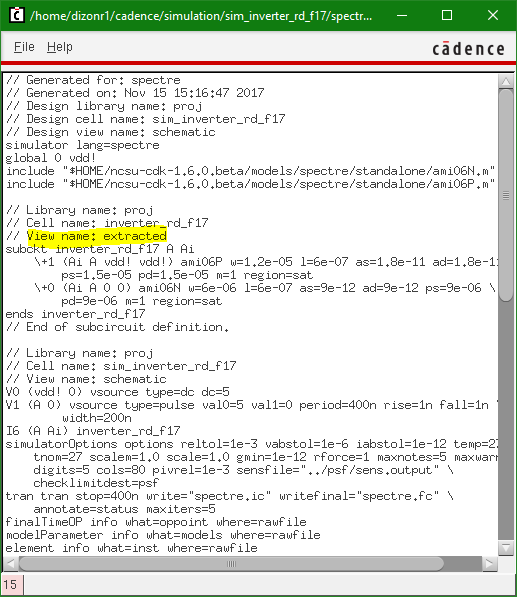
|
3) Layout of Even Parity Checker Circuit
For
this circuit, I tried to create a compact layout by placing four of XOR
gate layouts side by side for two rows to layout the eight XOR gates
necessary for the parity checker. The power and ground for each row is
tied together as well as the power and ground of each other. I placed
the power and ground pins for the entire circuit onto the first row of
vdd! and gnd!. Below the XOR gates, the inverter gate is laid out
closest to the output of the last stage of XOR gates. Finally, I added
the layout of the output pad and connected each of its pins onto the
corresponding connections (i.e. vdd tied to global vdd!, gnd tied
global gnd!). The input (data_out) is connected from the output of the
inverter gate, and the output of the circuit (check) is generated by
creating a pin onto RealOutput pin of the output pad layout. Here are
my layout and DRC results:
LAYOUT
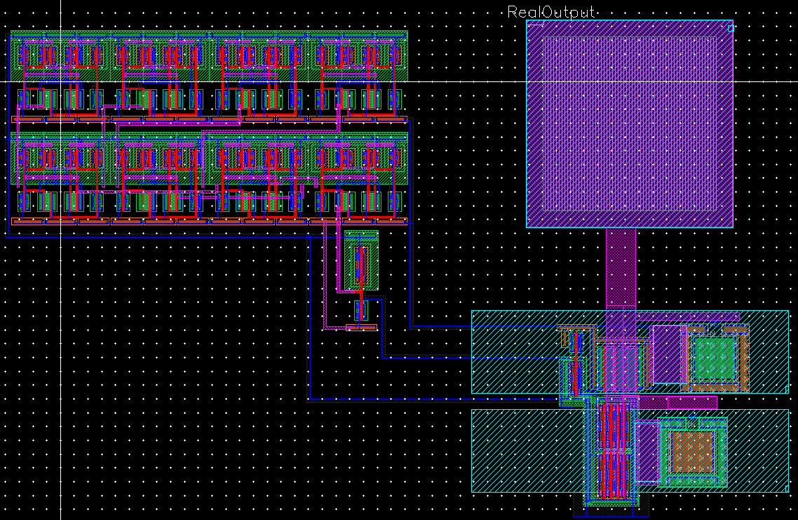 | DRC RESULTS
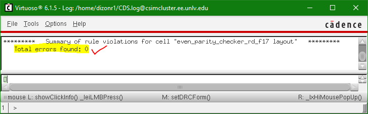
|
EXTRACTED LAYOUT
 | LVS RESULTS

|
EXTRACTED SIMULATION
 | NETLIST PROOF
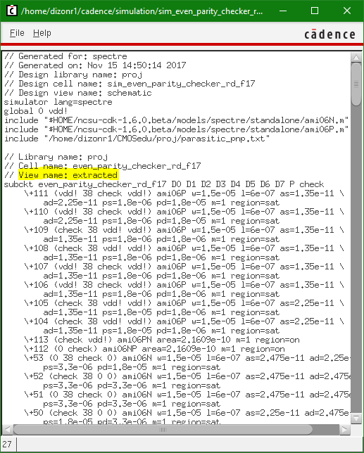
|
This concludes the lab final project. Below is the full design directory for this project:
Return
to Reiner's Labs
Return
to EE 421L Labs