Lab 3 - EE 421L
This
lab will focus on layout design for the 10-bit DAC from last lab. For
the prelab, I finished the rest of Tutorial 1 and backed up all of my
work for the lab and the lecture both from the csimcluster and the
website.
LAB REPORT
| How to select the width and length of the resistor: The sheet resistance of the n-well from MOSIS's information is about 800 ohms/square. With this information, we can determine the required length of a 10k n-well resistor assuming that the width is 4.5 microns. The calculation for length is as follows: |  |


After creating this n-well resistor layout, a Design Rule Check tool is used to determine if the design follows the rules for the process we are using. After successful check, the resistance value can be shown by extracting the layout which will show the value based on specifications of the process.

As seen above, the resistance of this n-well resistor is about 10.21K ohms.
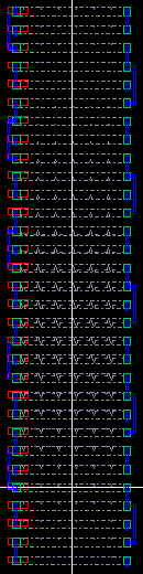
Layout View: This n-well resistor layout is the foundation to create the 10-bit DAC using 10k resistor. Here is my design of the 10-bit DAC and DRC results:
 | Zoomed In (at the bottom):   |
Extracted View: After finishing the layout, I extracted the layout to see the resistor values again and to compare it to the schematic using LVS.
 | Zoomed In: Extracted Results:
|
Layout vs. Schematic (LVS): With the extracted layout, I can now compare the layout to the schematic from lab 2.

Results:

Link to Design Directory Zip File
