Lab 2 -
EE 421L
Authored
by Reiner Dizon
Email: dizonr1@unlv.nevada.edu
Today's
date is September 12, 2017
Lab
description:
This
lab focuses on the design of 10-bit Digital-to-Analog Converter
(DAC) using n-wells for resistors. For the prelab, I simulated the
ADC to DAC circuit to ensure that it works and found out the
relationship between Vin and B[9:0] as well as Vout. In the lab, I made
a 10-bit DAC using 10k resistors which is turned into a symbol later on.
PRELAB
1) Narrative of prelab instruction
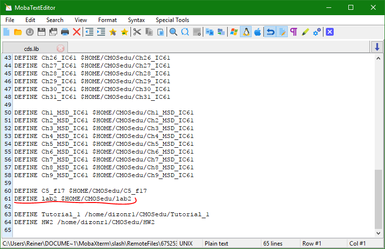
Step 1:
Download and unzip lab2 zip file from the Lab 2 instruction page onto
the CMOSedu folder in the csimcluster. Afterwards, add "DEFINE lab2
$HOME/CMOSedu/lab2" onto the cds.lib file.
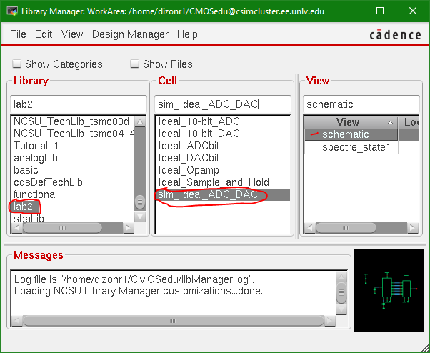
Step 2: After saving the cds.lib file and starting Virtuouso, the Library Manager will show the lab2 library.
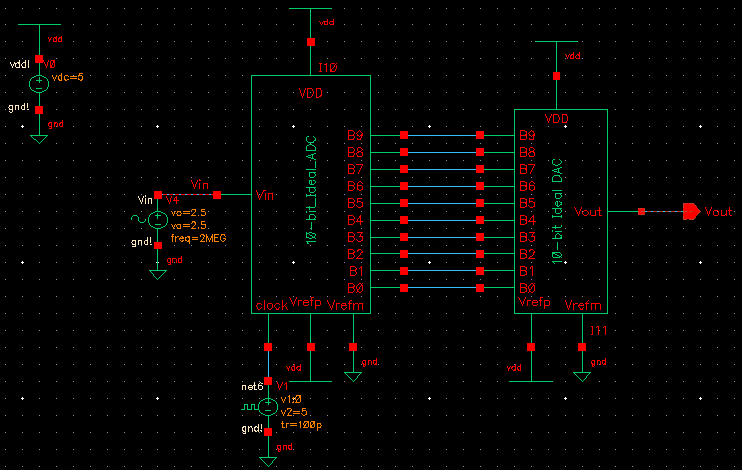
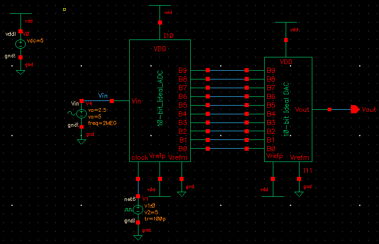
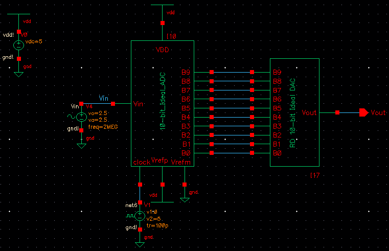
Step 3: Open the sim_ideal_ADC_DAC cell and the schematic.
Step 4: Simulate the transient analysis of the ADC-DAC circuit
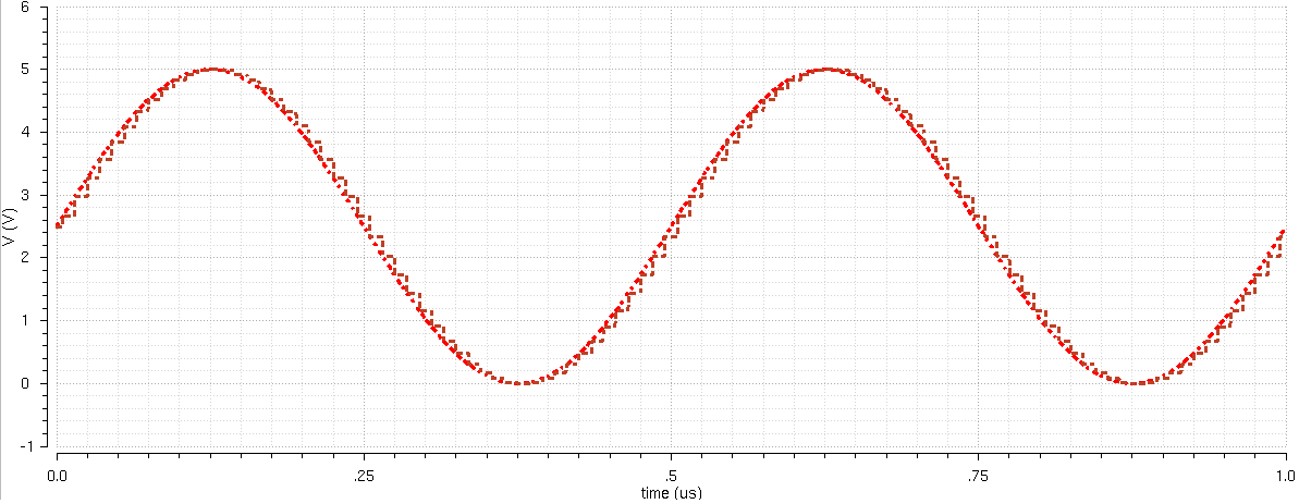
2) Discussion of ADC and DAC knowledge
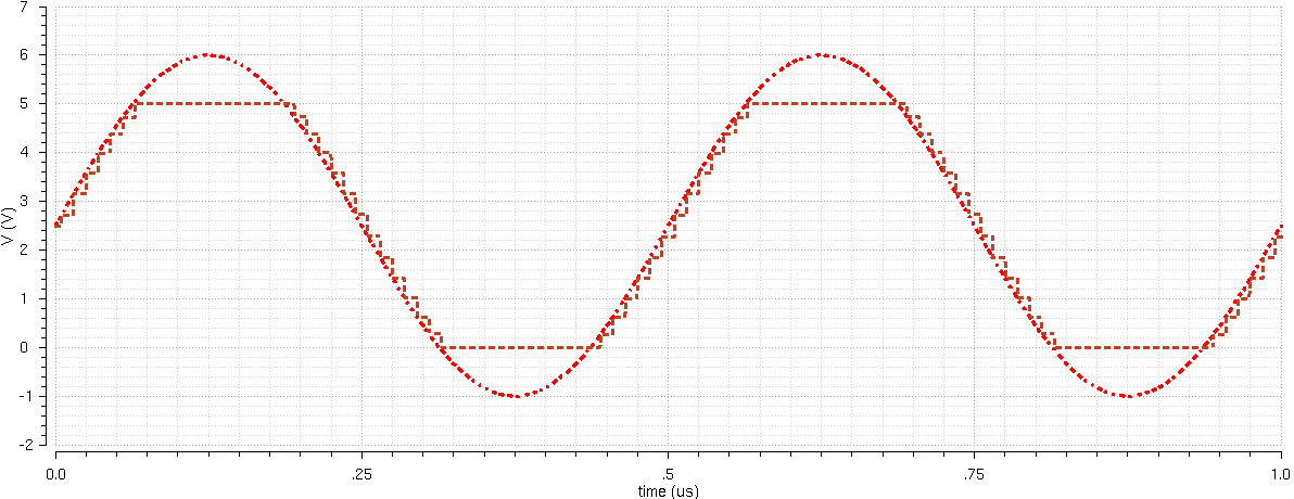
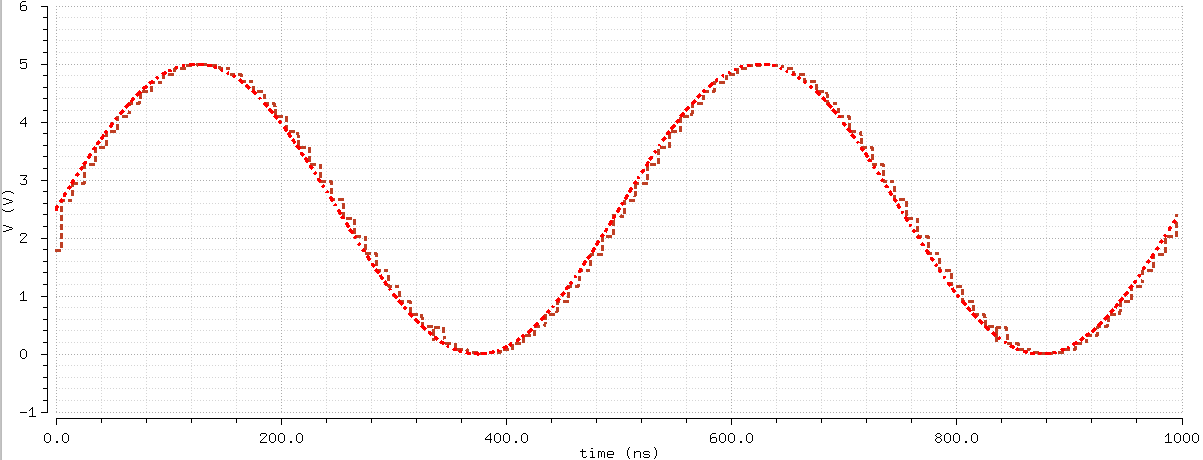
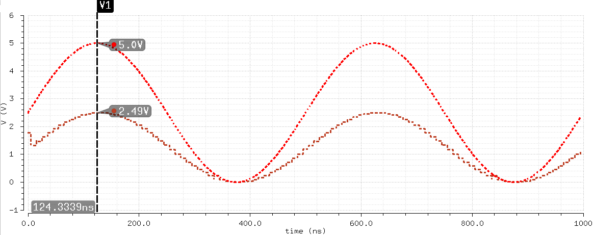
To demonstrate my knowledge of ADC and DAC, I changed the amplitude from 2.5V to 5.0V.
Simulation:
As seen in the simulation above, the voltage that can be read by the ADC is between 0 and 5 volts (the reference voltage).
Otherwise, the ADC will register the voltage as either 0V for any
voltage below 0V and 5V for any voltage above 5V. The decoding of the
digital values by the ADC is done using the DAC for which the output
voltage is measured from.
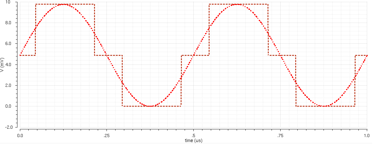
3) Explanation of how to determine LSB with simulation to support.
Because,
the converter is a 10-bit ADC, there are 1024 levels for voltages
between 0 and 5 volts (the reference voltage). The least significant
bit (LSB)
of the ADC is therefore the reference voltage divided by the total
number of levels or 2 to the power N, number of bits. Alternatively,
LSB = Vref / 2^N.
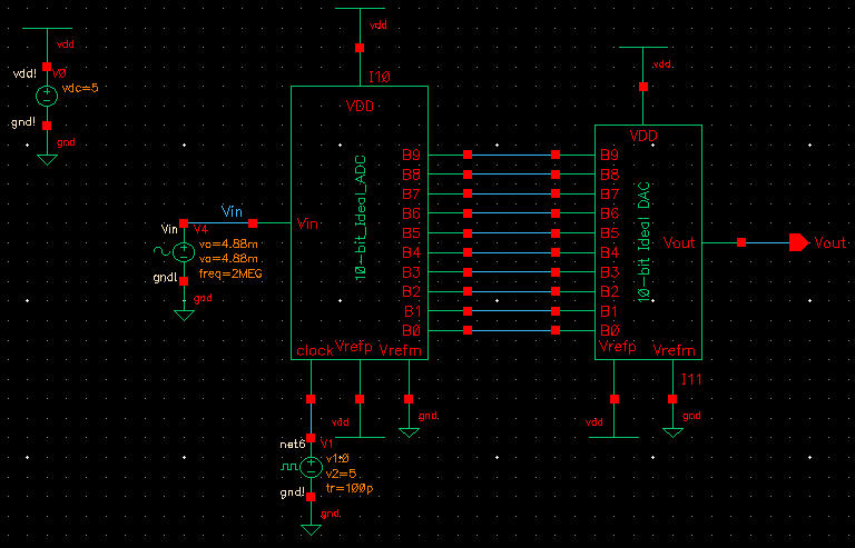
For this circuit, the LSB = 5V / 2^(10) = 4.88 mV. To verify this calculation, I changed the offset and amplitude to 4.88 mV.
LAB
REPORT
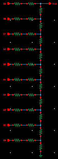
Design of 10-bit DAC using a n-well R of 10K ohms:
| Zoomed In:
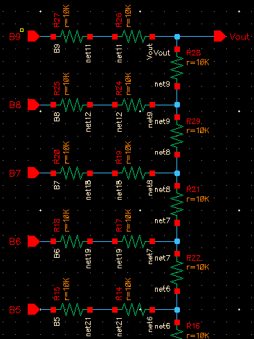
|
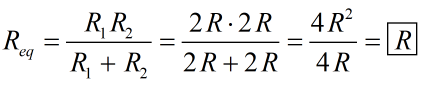
Determine the output resistance of DAC:
(1) The bottom two 2R resistor (circled in red) are in parallel, so they have an equivalent resistance of R because:
(2) After changing parallel 2R resistor into a single R resistor, this R resistor (circled in red) is in series with another R resistor, which can be combined into an equivalent resistance of 2R (circled in green). Again, this newly combined resistor of 2R resistance is in parallel with another 2R resistor.
Repeating these two steps will yield a final equivalent resistance of R.
Schematic with B9 connected to pulse signal and all other signal grounded: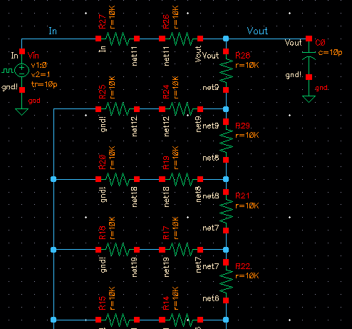
Since
the output resistance of the DAC is R, where R = 10K ohms, and
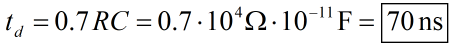
capacitance is 10 pF, the delay of the RC circuit is calculated as
follows:
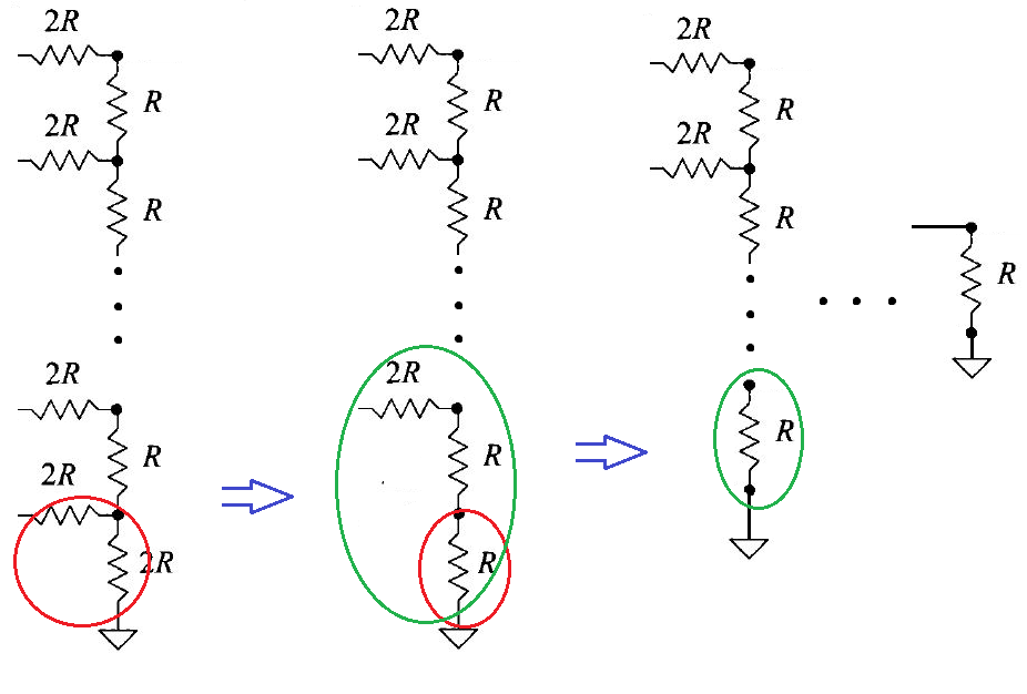
Simulation
Based on this simulation, time delay = 74.3174 ns - 5.0025ns = 69.3149 ns
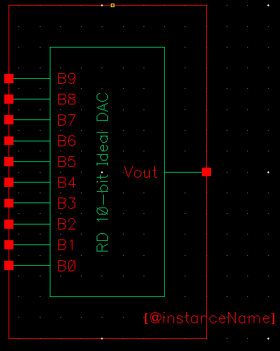
Create a new symbol for my DAC design: copy symbol from Ideal_10-bit_DAC to RD_10-bit_DAC and remove outside voltage pins.
Simulation of new design (above) by copying original simulation cell to sim2_Ideal_ADC_DAC:
ADC/DAC schematic with resistive load of 10K ohms: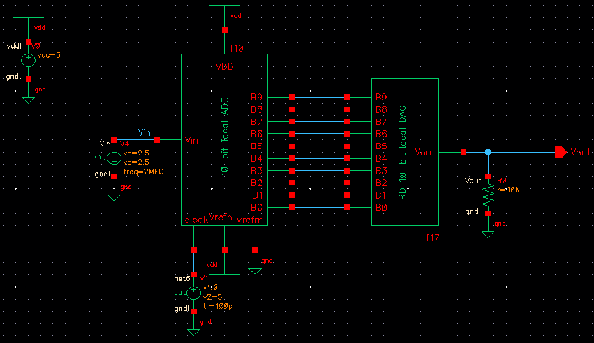
Simulation of this above circuit and answer to what happens to DAC driving a 10k load:
After
placing a 10k resistor to the output of the DAC, the output voltage
decreased by half since DAC's output resistance is 10k ohms which is in
parallel with the 10k load.
Therefore, this creates a voltage divider circuit. Since the max input voltage is 5 V, the max output voltage is about 2.5 V.
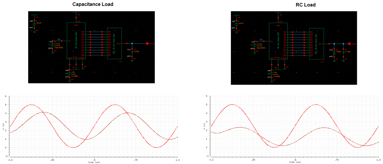
Simulations for capacitance load and RC load:
The
addition of a capacitor adds a delay on the output as seen in the
simulation above for circuit of both capacitive and RC loads.
What happens if the resistance of the switches isn't small compared to R:
The
resistance of switch in series with the 2R resistor has an equivalent
resistance higher than 2R. When applying series and parallel resistance
to the DAC resistors, the output resistance is less than R. This will
result a much lower output voltage.
Backup for Lab 2:
Return
to Reiner's Labs
Return
to EE 421L Labs