Project - ECE 421L
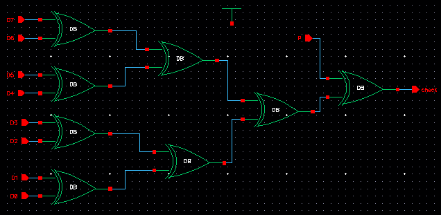
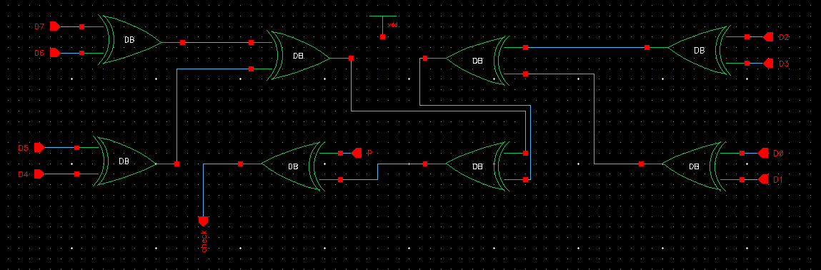
**(Note: the above schematic is used to aide in explanation, for actual implementation buses were used. (View Schematic) **
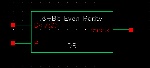
Symbol created for easier instantiation and simulations
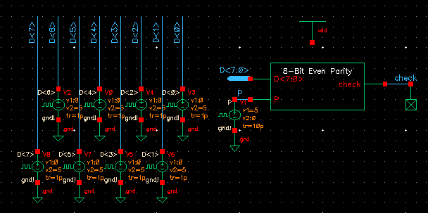
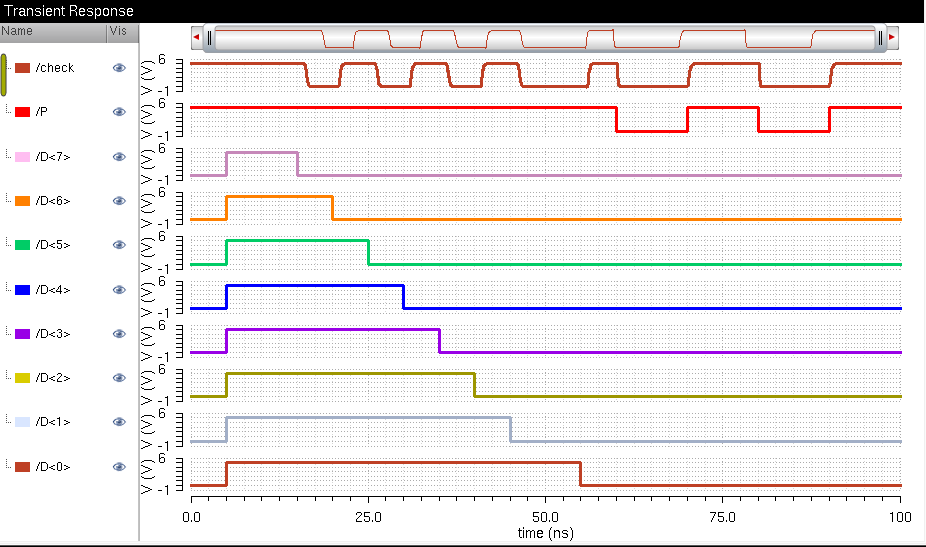
Simulation schematic and simulation results showing when P = 1 the check output = 1 when there are and even number of 1's on the data bus and 0 otherwise. (Click here to view a Simulation of ALL possible inputs)
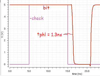
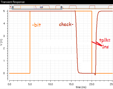
Zoomed in photos of the simulation results shows the fall and rise times of the check output when a data bit is changed.
tf = 1.3ns and tr = 1ns (note this includes the propagation delay from the multiple stages of XOR gates.
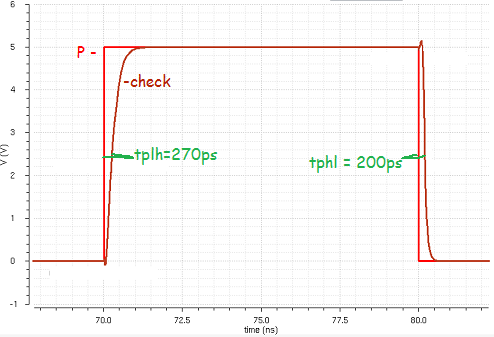
When the P bit is changed, we see much shorter rise and fall times of tr = 270ps and tf=200ps since it is directly
connected to the final xor gate.
Summary of rise/fall times
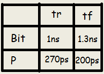
Looking back at the schematic, it makes sense that the rise time is longer for the single gate but the fall time is
longer when changing a bit. This is because when a bit is changed to set the output to 0 the first three xor gates
have to go to 1. When a bit is changed to set the output to 1 the first three xor gates are set to zero to set the
output to 1.
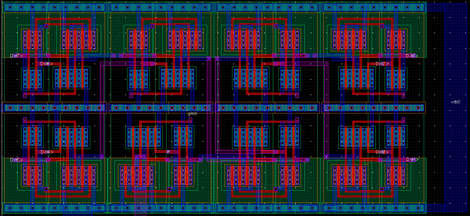
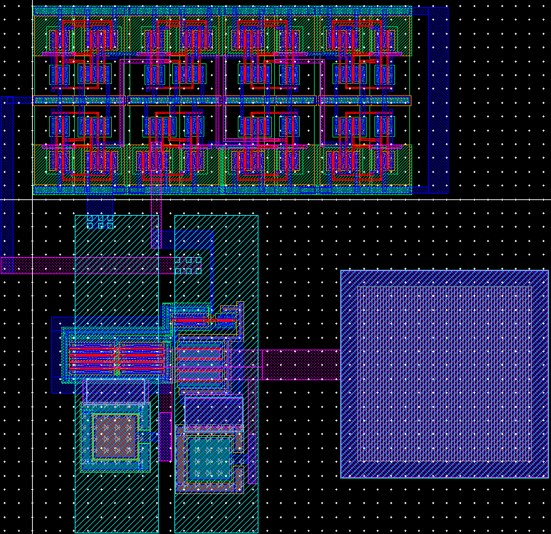
Part (II) Layout
For the layout I arranged the 8 nor gates as pictured above to make routing the interconnecting wires easier