Lab 08 -
EE 421L
12/06/2017
Generating
a test chip layout for submission to MOSIS for fabrication
Junho
Bae
baej8@unlv.nevada.edu
Desi
Battle
battled@unlv.nevada.edu
Jeeno
Doria
doriaj3@unlv.nevada.edu
(VDD = 5 V)
This
Chip contains the following:
- A 31-stage
ring oscillator with a buffer for driving a 20 pF off-chip load
- NAND gate using 6u/0.6u NMOS and PMOS
- NOR
gate using 6u/0.6u NMOS and PMOS
- An inverter
made with a 6u/0.6u NMOS and a 12u/0.6u PMOS
- Transistors,
both PMOS and NMOS, measuring 6u/0.6u
- A 25k resistor
implemented using the n-well
- A voltage
divider using the 25k resistor laid out above and a 10k resistor
- An even partiy
checker 9-bit input word (8-bits data & 1 bit parity), 1 output
Cadence design directory: Chip5_f17 (click to download)
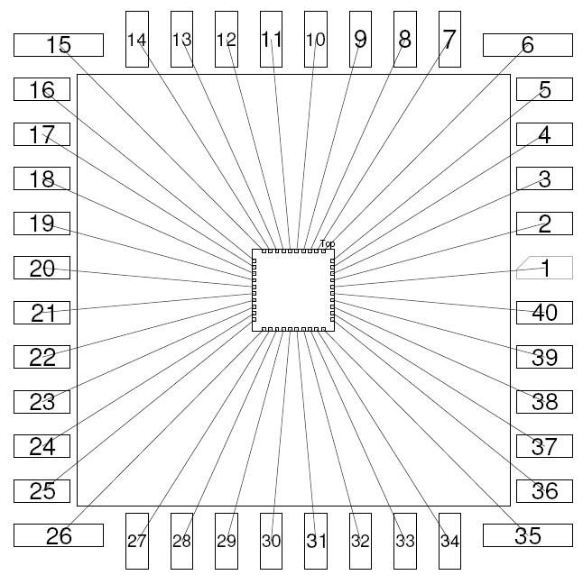
Pinout Overview


Chip Schematic & Layout
| Chip Schematic | Chip Layout |
 |  |
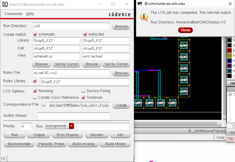
| DRC | LVS |
 | 
|
Pinout Detailed
NMOS
PMOS


Drain:
Pin<18>
Source: Pin<15>
Gate:
Pin<17>
Gate: Pin<13>
Source: Pin<19>
Drain: Pin<14>
*NMOS
body tied to ground (pin 20)*
Body: Pin<16>
Test Instructions: (configure as inverter)
Connect Pin <15>, Pin<16> to VDD
Connect Pin<19> to Pin<20>
Connect Pin<14> to Pin<18> (short the drains)
Connect Pin<17> to Pin<13> (short the gates)
Apply square wave to Pin<13> and observe Pin<19> is inverted
NOR

Inputs: Pin<7> and Pin<8>
VDD: Pin<10>
Output: Pin<9>
Test Instructions:
Connect Pin<10> to VDD
Connect Pin<7> and Pin<8> to all 4 possible combinations of 0,VDD
observe Pin<9> is correct
NAND

Inputs: Pin<3> and Pin<4>
VDD: Pin<6>
Output: pin<5>
Test Instructions:
Connect Pin<6> to VDD
Connect Pin<3> and Pin<4> to all 4 possible combinations of 0,VDD and observe
Pin<5> is correct
Inverter

Inputs: Pin<21>
VDD: Pin<23>
Output: Pin<22>
Test Instructions:
Connect Pin<23> to VDD
Apply square wave to Pin<21> and observe inverted output wave
Ring Oscillator

VDD: Pin<2>
Output: Pin<1>
Test Instructions:
Connect Pin<2> to VDD
Connect a 20pF(max) capacitor between Pin<1> and Pin<20> (ground
Observe output oscillates with
Voltage Divider

Input: Pin<11>
Output: Pin<12>
Test Instructions:
Connect Pin<11> to known voltage
measure Pin<12> (Out = 0.7In)
Even Parity Checker

Inputs: Pin<24:31> (Data) and Pin<32> Parity(P)
Output (check): Pin<33>
VDD: pin<34>
Even Parity Checker operation
9-bit input word, 8-bits data and 1-bit parity, that outputs a 1 (0) when the even parity check is valid (invalid)
Test Instructions:
Supply VDD (5V) to pin<34>
Ensure all input pins are either grounded or tied to VDD and observe output is correct
No Connection

Pins <35:40> are unused
Test Instructions:
Stare blankly at chip.
Return
to EE421L Labs


