Lab 6 - ECE 421L 

Authored by Desi Battle,

battled@unlv.nevada.edu

10/25/2017


                For lab 6 we are tasked with implementing two logic gates, XOR and NAND as schematics as well as layouts then using those gates to implement a full-adder.


StdFrame.JPG

To prepare for the layout portion of the lab, first I laid out a standard cell frame.  

This provides us with a predefined area to lay out our PMOS and NMOS device 

as well as VDD and ground rails lining the top and bottom of the frame respectively.  

If we need more space we can quickly paste copies of the frame horizontally.


DigitalInput.JPG

For this lab we also configure vpulse sources to act as our digital inputs when we test the components.

It is important the Rise and Fall times are << Pulse width or we will see unexpected behavior when the inputs switch.


nand2/nand2_01_schematic.JPG       nand2/nand2_02_symbol.JPG

                                                shchematic for NAND gate and corresponding symbol


nand2/nand2_03_layout.JPG        nand2/nand2_05_extracted.JPG 

                                                                         DRC RESULTS                                                                                                                LVS OUTPUT

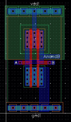
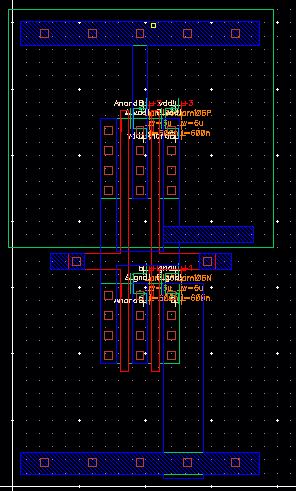
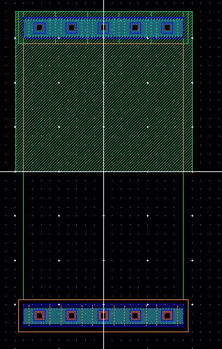
                                                NAND gate layoutand Extracted view. A LVS was performed to be sure our layout and schematic matched. 


nand2/nand2_07_symbolsim.JPG            nand2/nand2_08_sim.JPG

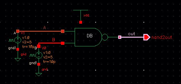
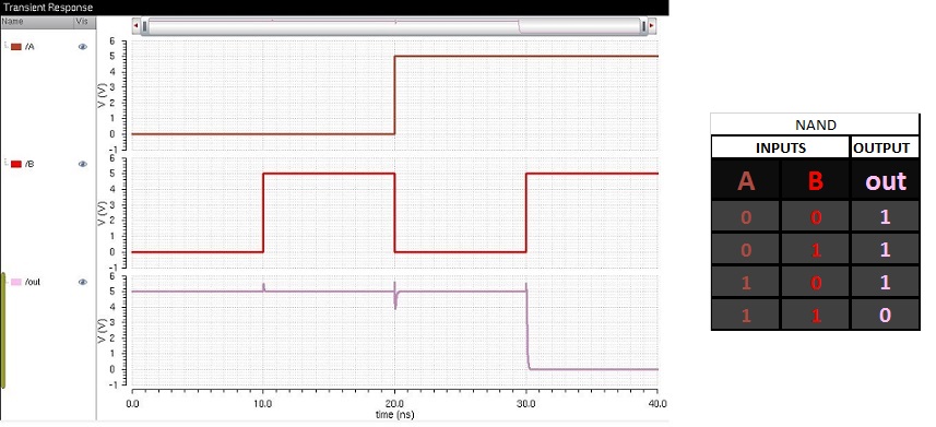
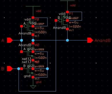
Next I instantiated the NAND symbol made earlier and used pulse sources as discussed in the beginning of the lab to simulate and verify our design.


xor2/xor2_01_schematic.JPG        xor2/xor2_02_symbol.JPG

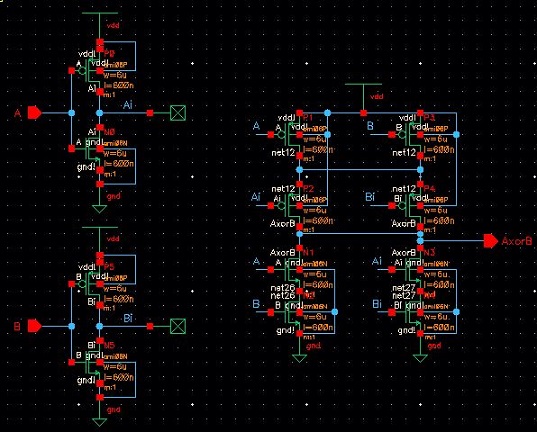
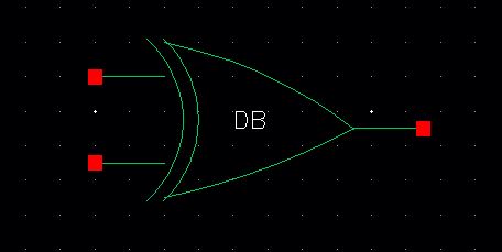
Next, I drafted the provided schematic for an XOR gate and made the corresponding symbol


xor2/xor2_03_layout.JPG    xor2/xor2_05_extracted.JPG

                                                                            DRC RESULTS                                                                                                                                 LVS OUTPUT
 

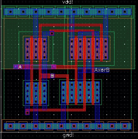
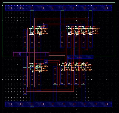
                                            The XOR gate layout was quite a bit more challenging than the NAND gate simply due to the increase in transisters required.

                                                                         In the more crowded areas I used and metal2 to ease the difficulty of the layout.


xor2/xor2_07_symbolsim.JPG    xor2/xor2_08_sim.jpg

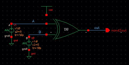
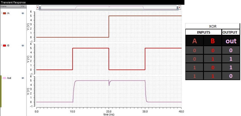
Again our symbol was instantiated with pulse sources to run a simulation to confirm our gate is working as designed.


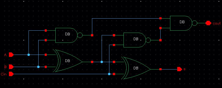
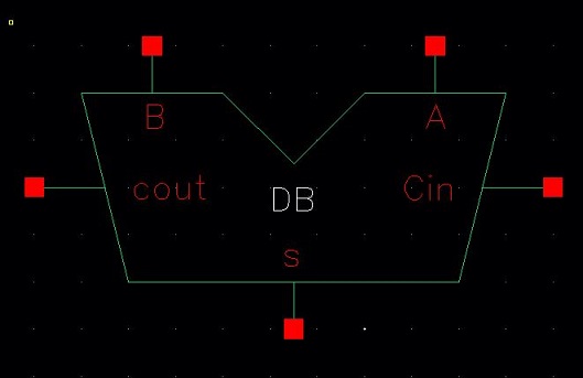
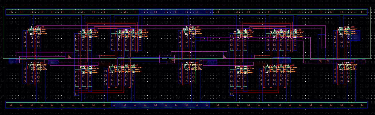
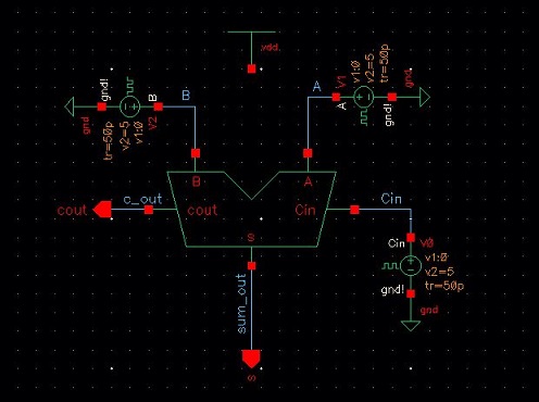
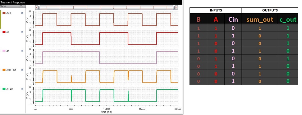
The last part of the lab required us to use the two gates created in the first two parts of the lab to implement a Full-adder.

fulladder/fulladder_01_schematic.JPG        fulladder/fulladder_02_symbol.JPG

I implemented the provided schematic with my gates and drew my best interpretation of the full adder symbol.


fulladder/fulladder_03_layout.JPG
                                                                                                                                                                                    DRC RESULTS

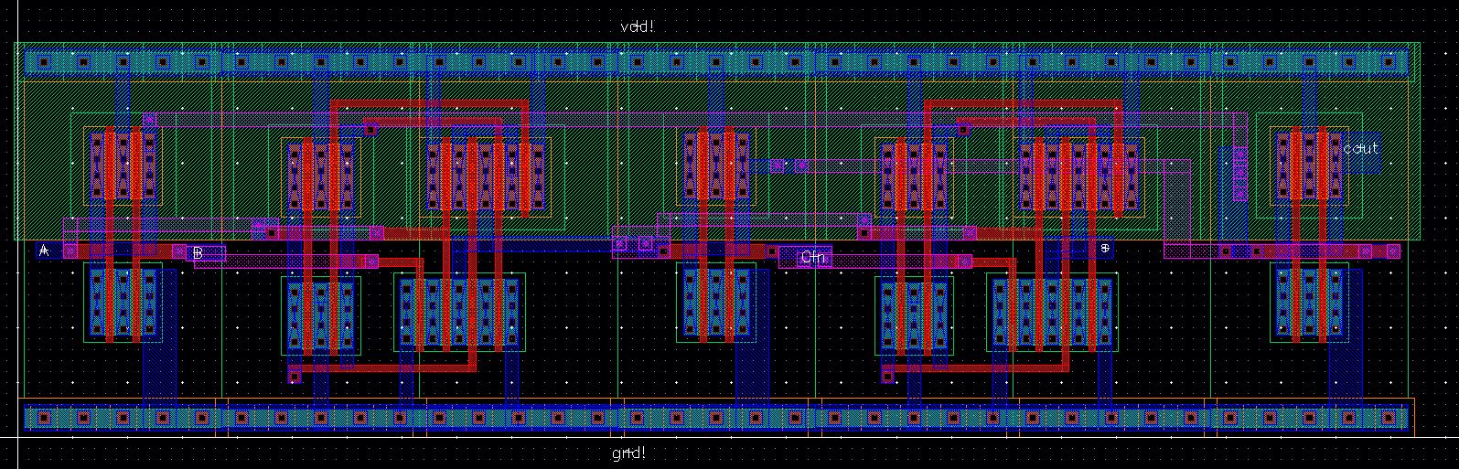
                                        For the layout of the full adder I used metal2 much more liberally to avoid having to route around

                                        metal1 and poly. At this point I realized my standard cell frame probably should have been taller, 

                                         because anything larger than the full adder would almost certainly not fit in my frame. 


fulladder/fulladder_05_extracted.JPG

                                                                                          Extracted  view and   LVS RESULTS


fulladder/fulladder_07_symbolsim.JPG            fulladder/fulladder_08_sim.jpg

Again our symbol was instantiated with pulse sources to run a simulation cycling through all possible digital inputs to confirm our fulladder is working as designed.


Click the link to download a zipped up copy of the library created for this lab report: ---> lab6.zip <-----


Return to other EE421L students labs

Return to My Labs