Lab 5 - ECE 421L
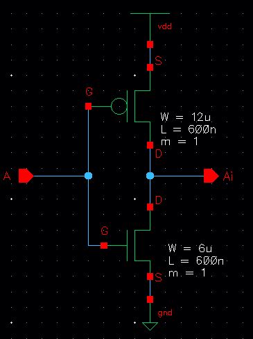
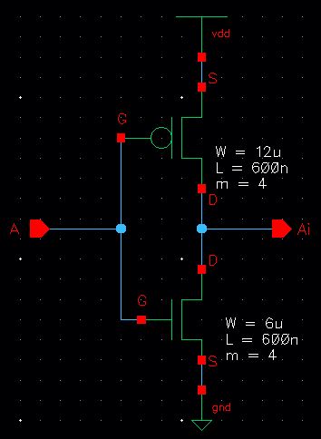
Schematic of the two inverters studied for this lab. the sizes of the PMOS are 12u/600n and the NMOS are 6u/600n.
The only difference between them is that a multiplier of 4 is applied to the NMOS and PMOS on the right.
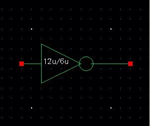
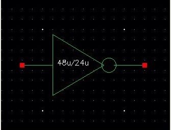
Next symbols were created for each schematic with text labels to denote the sizes.
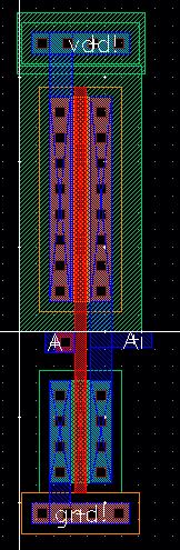
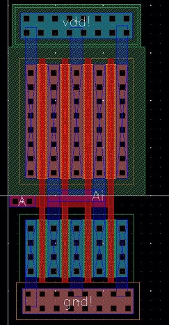
Next I created layouts for both inverters. Once they were completed I ran a DRC on each and extracted
them so they can be LVSd. (See above links for DRC results).
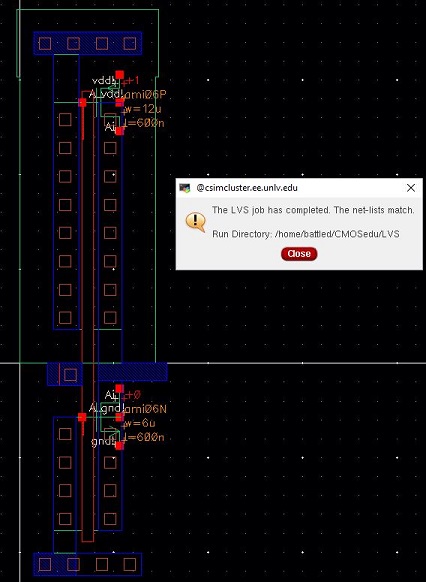
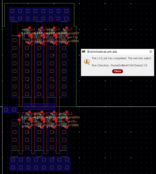
After extracting the devices I ran an LVS to confirm the net-lists were matching. (See above links for full LVS output)
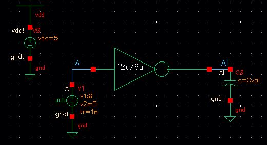
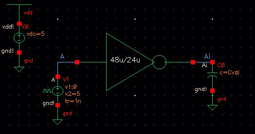
At this point schematics were drafted to simulate each inverters response to a pulse source with varying capacitive loads.
By setting C = Cval on the schematic, I am parameterizing my simulations to view the output of different loads simulteanously.
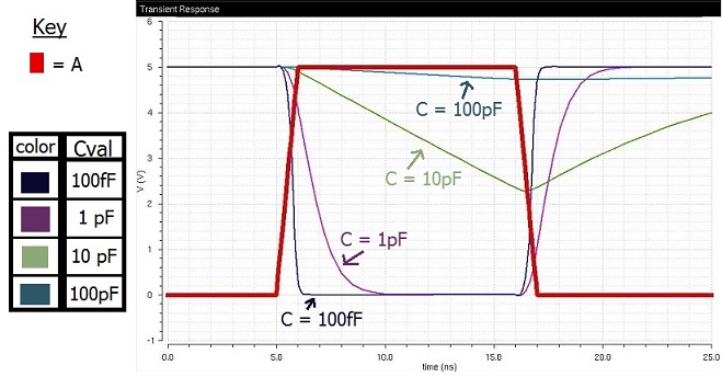
Seeing the outputs relative to eachother better demonstrates the effect changing Cload has on the circuit.
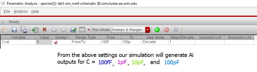
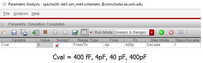
Parametric Analysis settings to configure Cval for our simulations as mentioned above.
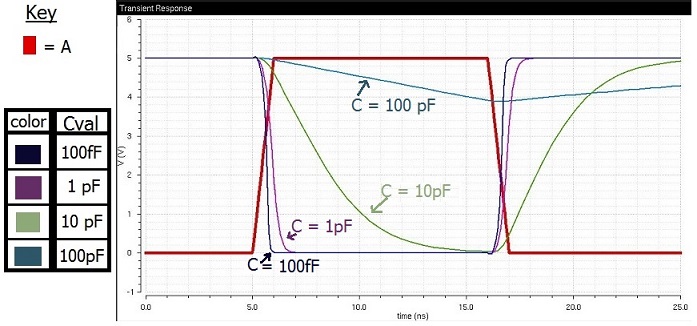
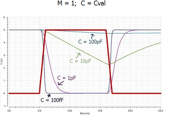
Single nmos/pmos inverter simulation results Four nmos/pmos inverter simulation results
For both cirucits simulated, the output of the devices are limited in their ability to change with the input by their slew rate. (slew rate = dV/dt = I/Cload).
From this equation it is obvious why as Cload is increased, the circuits ability to follow the changing input signal is hindered further. The next most notable
observation is the increased performance when using 4 nmos/pmos instead of just one. While each transistor does add small capacitances between the
layers, that parasitic effect is overwhelmed by the fact that 4 transistors can source 4 times the current of one transistor. To verify that this is
indeed the case, I ran one more simulation on the sim_not4 schematic with load capacitances 4 times the size of the previous simulation to see if the
effects of the four transistors are canceled out by the effects of having to source current to four times the load.
Parametric analysis settings to increase Cload by a factor of 4.
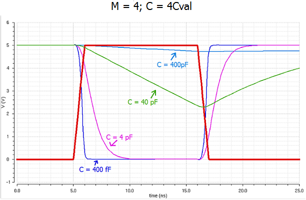
Simulation results from single nmos/pmos inverter Simulation results from four nmos/pmos inverter with four times the load
The waveforms now look identical since the increase in the current able to be supplied is matched by a proportional increase in current demanded.
In general increasing the number of transistors in this design has some pretty straightforward trade-offs. Your circuit will be faster since you will source more current and
thus have a higher slew rate. But that also means your design is larger and draws more power. These trade-offs should be kept in mind when trying to decide how many NMOS/PMOS
devices should be used for a design.
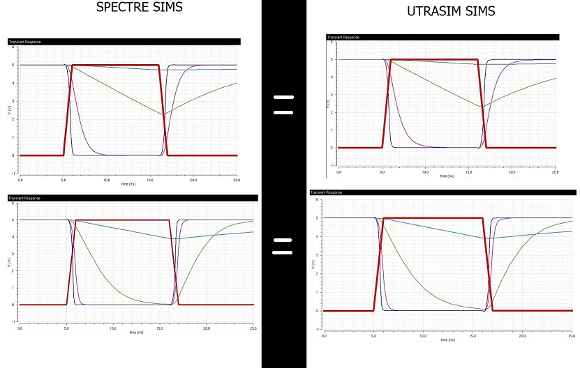
Per the labs instructions, I performed the simulations using Spectre and then again with Ultrasim. I could not see any
difference in the results so I just used the Spectre simulations throughout the report.
Click HERE to download the Cells used in this report