Lab 4 - ECE 421L
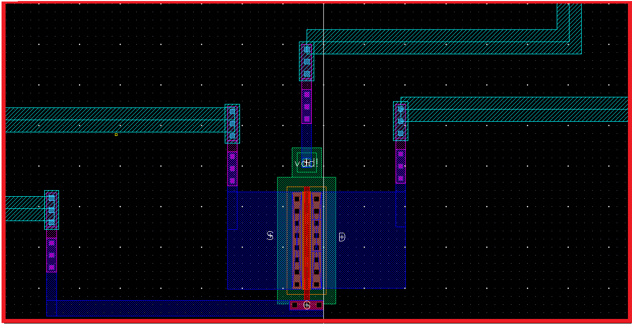
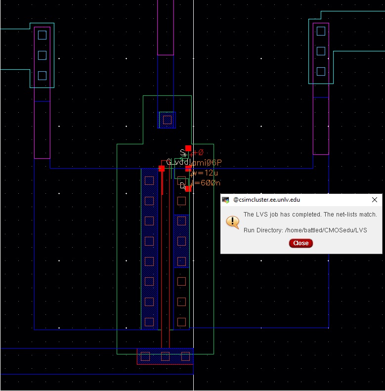
ALL NMOS devices have their body terminal tied to ground and ALL PMOS devices have their body tied to VDD = 5V. To simplify drawing the schematics
I made symbols for NMOS and PMOS devices where their bodies are already connected to ground and VDD respectively that will be handy for the vast
majority of layouts created in this course.
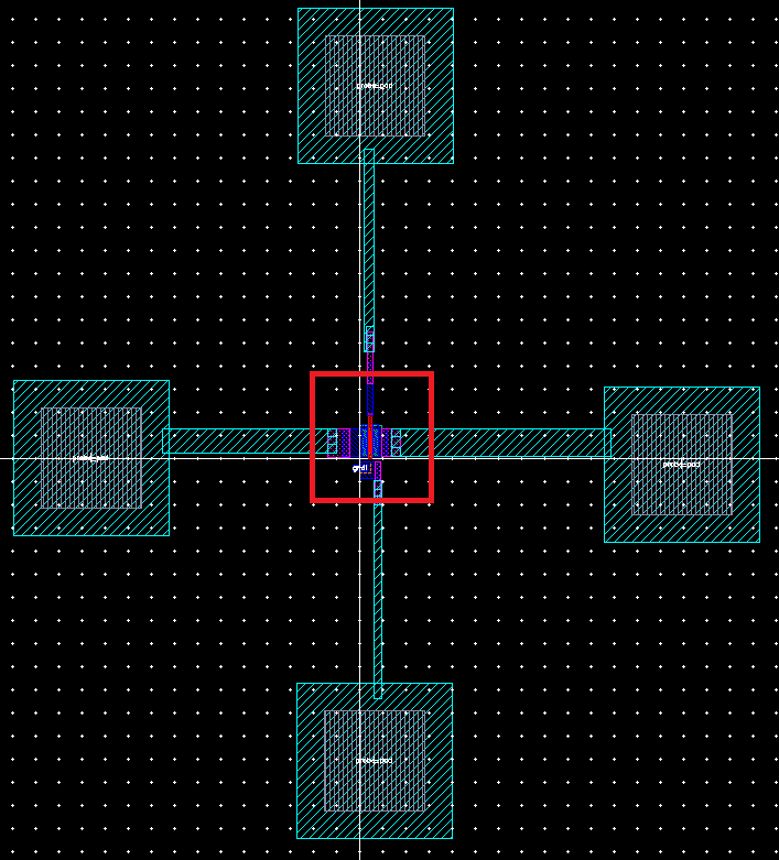
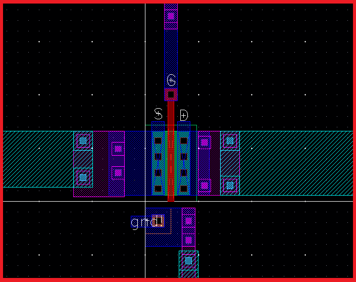
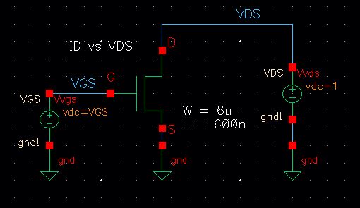
Schematic for testing NMOS drain current ID vs VDS for different VGS
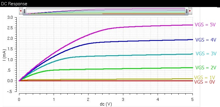
Here we see the results of our simulation. VDS is swept from 0 to 5 in 1mV steps and the resulting current is plotted for VGS = 1, 2, 3, 4, 5
Notice how when VGS is less than the threshold voltage the changing VDS has no effect.
It is also worth noting that we see a steep increase in ID as VDS increases until VDS = VGS+Vthn; when the device becomes saturated
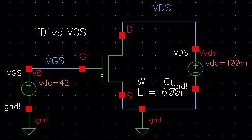
Next we made a schematic for testing ID as VGS is swept and VDS is held constant
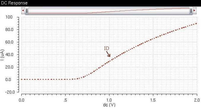
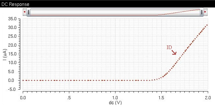
The simulation results of keeping VDS at a constant 100mV while VGS is swept from 0 to 2 V in 1mv steps are shown above.
Around VGS = 800mV we can see the device start to draw rapidly increasing current until the device beings to enter the
triode region as VDS becomes less than VGS - Vthn; hindering the devices ability to draw more current.
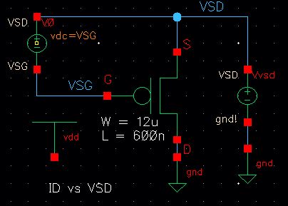
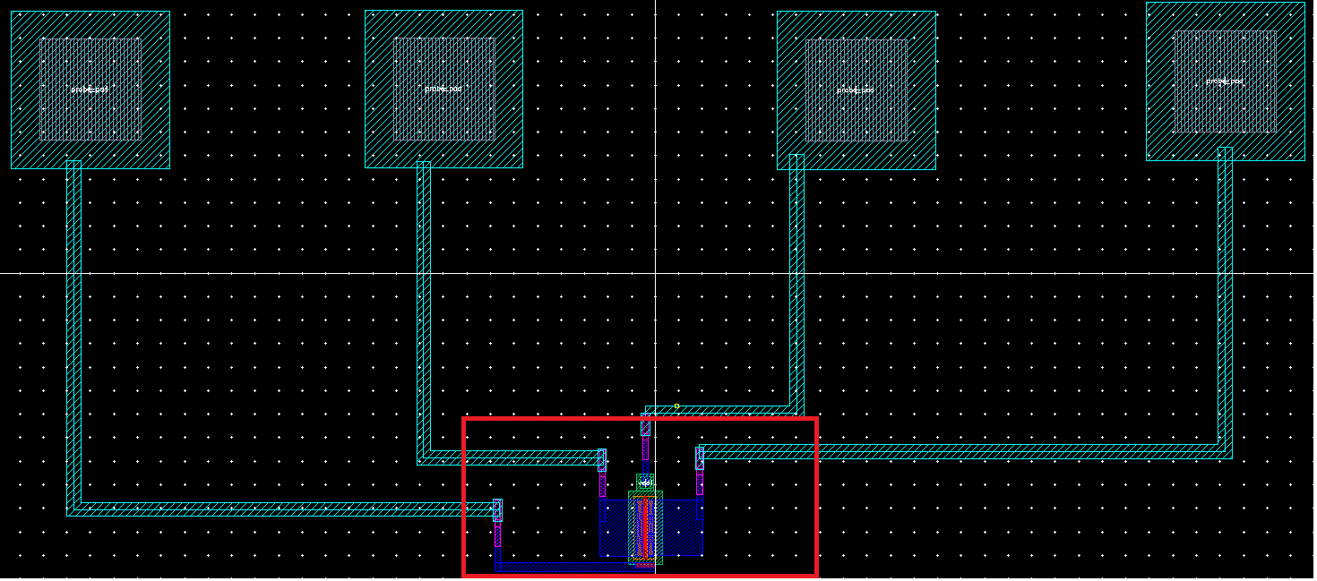
Schematic for testing PMOS drain current ID vs VSD for different VSG
Here we see the results of our simulation. VSD is swept from 0 to 5 in 1mV steps and the resulting current is plotted for VSG = 1, 2, 3, 4, 5
Notice how when VSG is less than the threshold voltage the changing VSD has no effect.
It is also worth noting that we see a steep increase in ID as VSD increases until VSD = VSG+Vthp; when the device becomes saturated
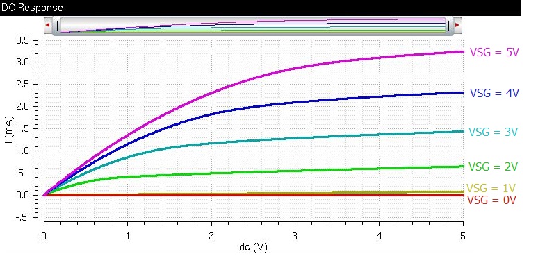
The simulation results of keeping VSD at a constant 100mV while VSG is swept from 0 to 2 V in 1mv steps are shown above.
Unlike the nmos, which turned on at about 800mV we do not see any increase in ID until about VSG = 1.5 V.