Lab 03 - ECE 421L
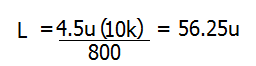
To begin the layout of our 10-bit DAC designed in lab 2, first we need to determine how to layout the individual 10k resistors
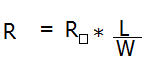
For our process we know that the n-well layer has an approximate resistance of 800ohms/square, and our minimum width is 12*lambda or 3.6um (lambda = 300nm)
Substituting using R= 10k, W = 4.5u (the width of ntap with 2 contact rows) , Rsq = 800 and solving for L gets us..
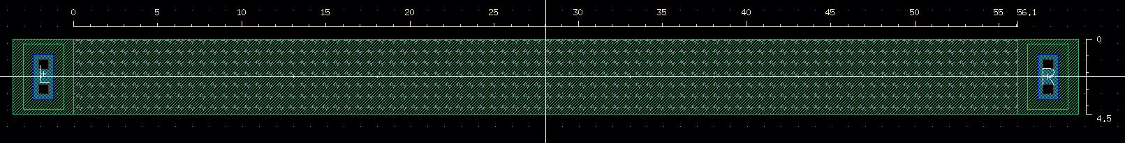
After laying out the resistor I used rulers to measure my W and L. The W matched exactly but the L came out to be slightly shorter than 56.25 at 56.1.
Being 0.15 microns shorter that I originally planned is fine since I was approximating to begin with.
Before
going any further, I made sure my resistor will be able to fit neatly
on the grid by dividing W and L each by the distance between grid
points (0.15), ensuring the result is an
integer. Otherwise, DRC will fail due to being off grid.
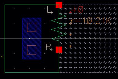
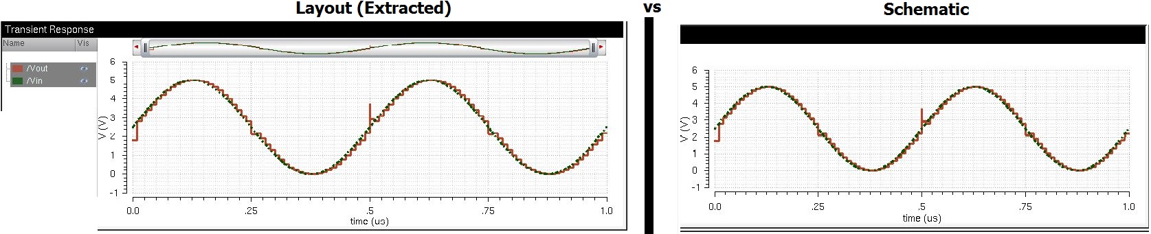
Here the extracted view of the layout above is pictured to confirm the resistor is approximately 10k. It is a little higher than I would like, but since our R-2R topology is more
dependent on the resistors all being the same value rather than precisely 10k, I can use exact copies of this cell without too much harm.
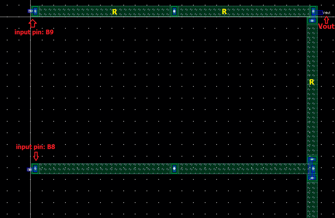
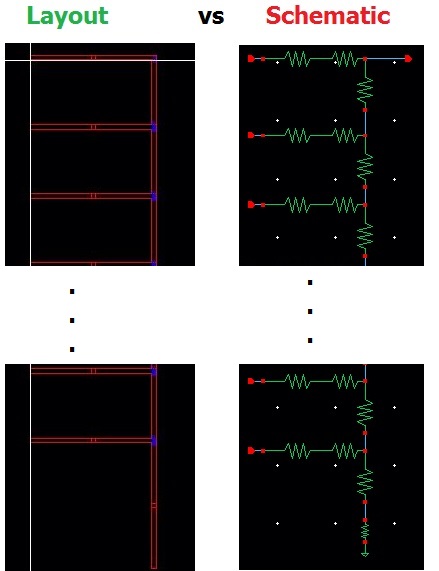
Using the previous layout as a template I connected the 10k n-well resistors in an R-2R topology. After I connecting B8, I did
a DRC to verify I did not break any rules I was unaware of, deleted B8, and used the F3 option when copying to copy 9 rows of bits at once.
After that was complete I only had to add the bottom 10k resistor, input pins, Vout, and gnd to complete the layout.