Lab 02 - ECE 421L
Authored
by Desi Battle,
Battled@unlv.nevada.edu
September 13, 2017
This lab covers ADC and DAC operation as well as the design of a DAC using n-well resisters.
Prelab
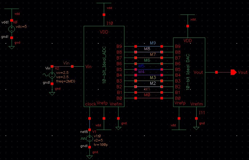
Provided schematic of 10-bit ADC and 10-bit DAC
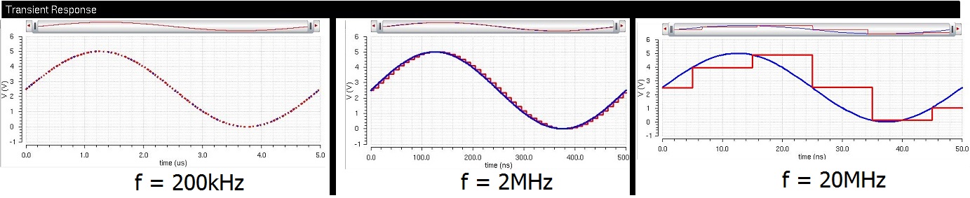
Transient
simulations of the above circuit with different frequencies show that
as frequency is increased on the input the error seen on the output
increases in severity. This is due to the fact that the DAC sampling
rate appears to be a canstant 10 ns, and the increase in frequency
causes the input to change more drastically in the given period.
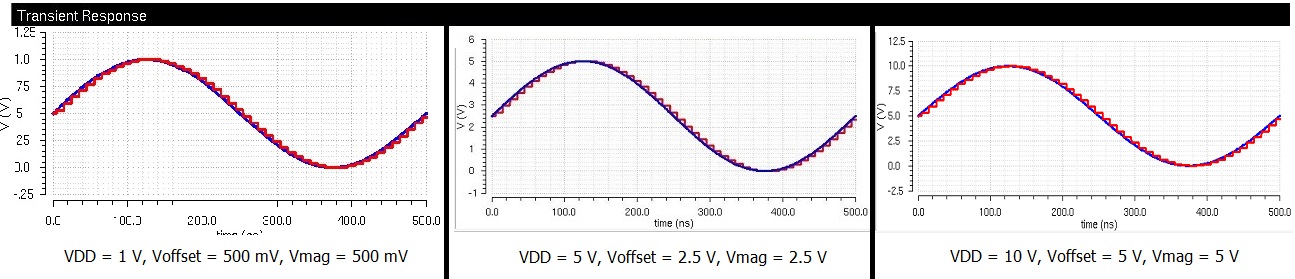
More
transient simulations done to observe differences when input signal is
changed. The waveforms are identical in shape because the
although input magnitudeis different for each
simulation,
it is always centered at Vref/2 and swings from 0 <-> VDD (VDD =
Vref). Since the relationship between Vref and Vin is maintained,
so is the waveform shape.
For this lab we will design a 10-bit DAC using a R-2R topology.
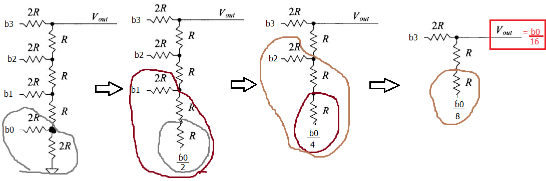
The
above is an example of a 4-bit example of the R-2R topology. The
derivation of b0's contribution to Vout by finding a Thevenin
equivalent is shown here.
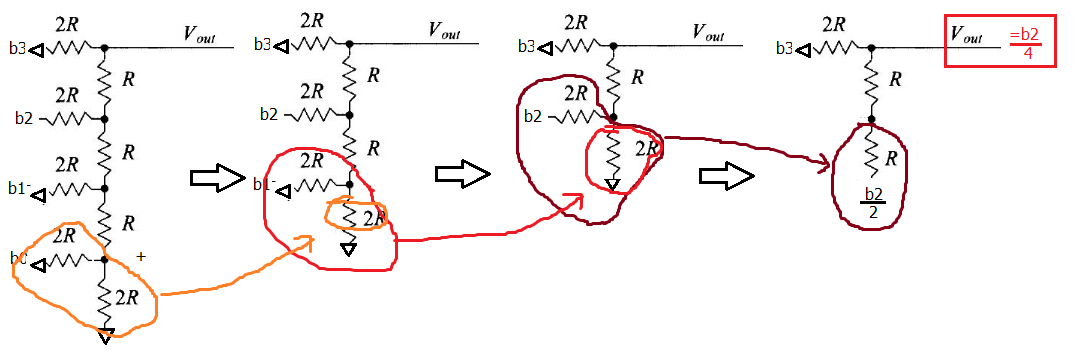
Here, for the same topology, b2's contribution can be derived by combining resistors and thevenizing.
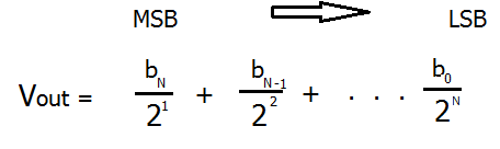
In general, by using superposition, we can see that for an N-bit R-2R ladder, Vout can be calculated as above.
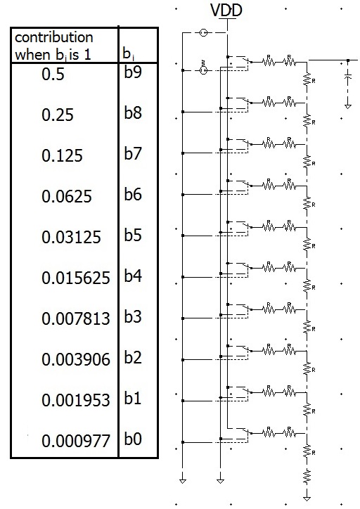
10-bit DAC schematic using R=10K
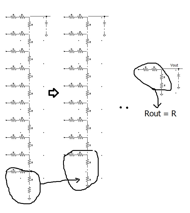
The
output resistance can be easily found by starting at the bottom bit and
combining parallel resistors until a solution is reached
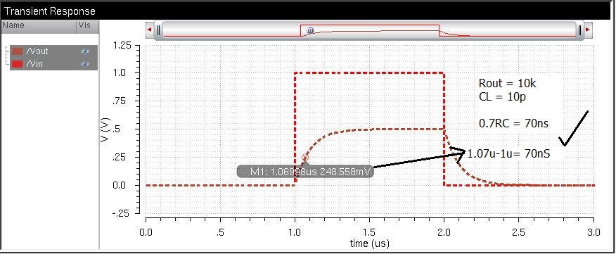
Above is a transient simulation done to verify rise time matches our calculation using 0.7RC
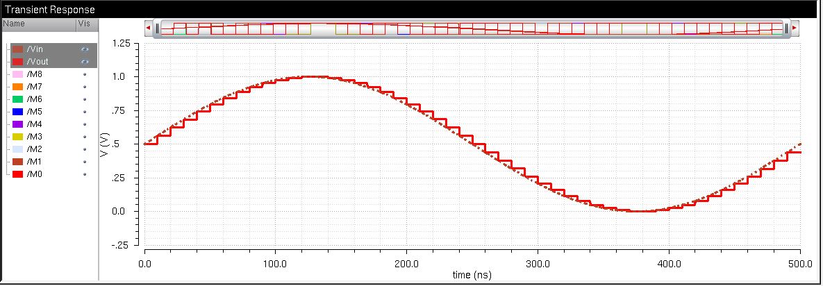
Transient simulation of MyDAC with no load working as desired
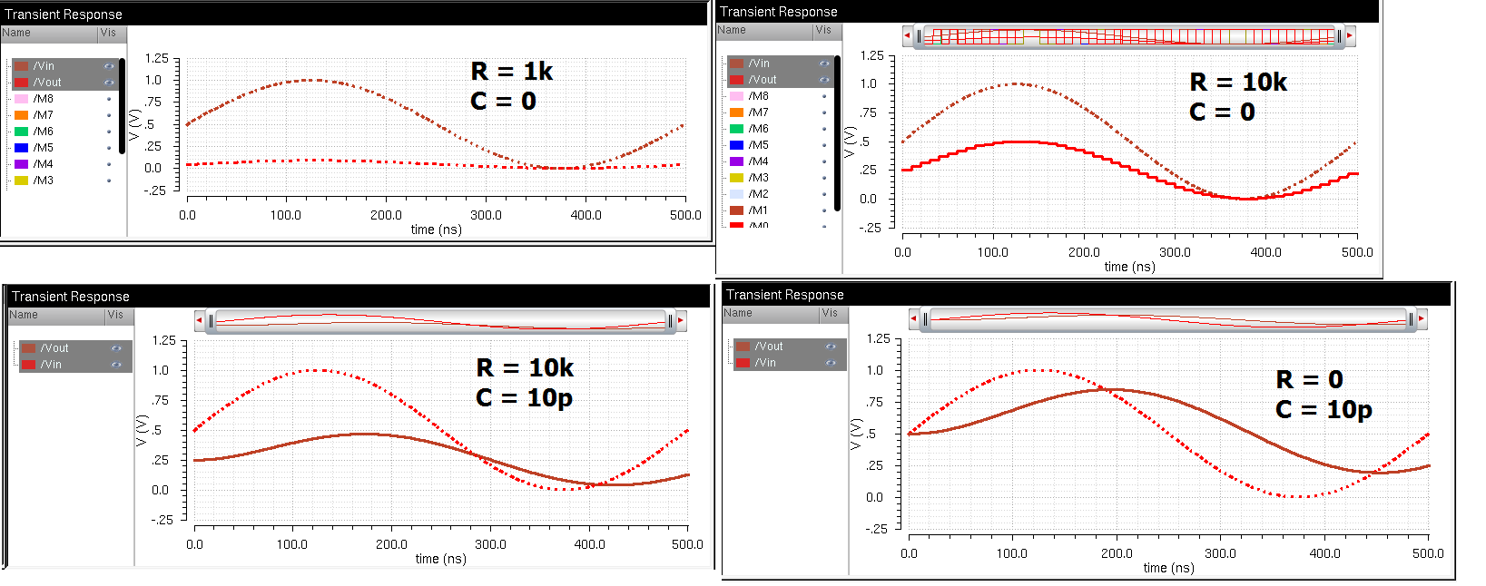
Next I simulated the DAC with varying loads to observe the effects of driving a resistive, capacitive, or mixed load.
For
the first sim I used a 1k resistor alone and could see the signal was
heavily attenuated due to 1k << 10k (the output resistance of the
DAC).
When
I increased R to 10k for the next sim, it is in parallel with the 10k
Rout of the DAC, causing the output be half of what it would
normally be.
Since R draws less current as it is increased, it
attenuates the signal less and less the bigger it gets until it is
essentially an open having no effect.
If
transistors were used to implement this design, they must have a
much output resistance than the 10k used in the ladder or they will
draw current and attenuate the signal similarly to a load resistor.
Then
I added a 10p capacitor with the 10k resistor and observed a phase
shift due to the inherit nature of the component. When both
resistive and capacitive loads were used the effects of each were
additived and lead
to
an attenuated, phase delayed output. The capacitive load alone
simply caused a phase shift and a slight loss in magnitude.
Return to my EE 421L Labs