Lab Project - EE 421L 

Authored by Junho Bae

baej8@unlv.nevada.edu

Schematic: November 15, 2017 

Layout: November 22, 2017


Project Description

   
A parity checker is used to check that the data that has been transmitted was accurate. This is done by adding a parity bit to the end of the binary code.

The goal of the project is design a even parity checking circuit that outputs a 1 when the total number of input bits that are '1' are even, and outputs a 0 if they are odd. 

The circuit will have 9 input bits (8-bits of data and 1-bit parity) and 1 output bit. 


The Schematic


The final even parity checking circuit is composed of XOR and XNOR gates, hence I will cover these two logic gates beforehand.


    Designing a 2-input XOR gate


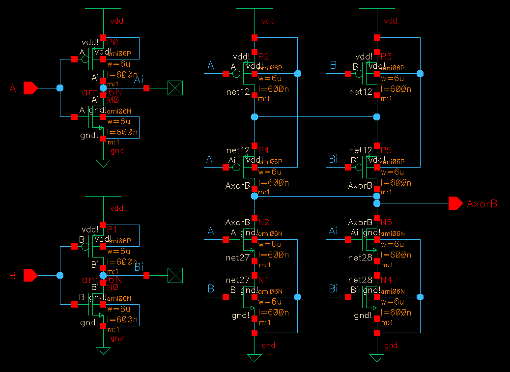
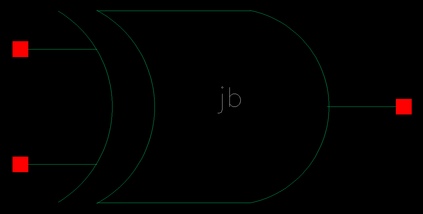
First I created a schematic and a symbol for the commonly used XOR gate. Below are the images of the XOR gate.


Schematic Symbol
http://cmosedu.com/jbaker/courses/ee421L/f17/students/baej8/proj/images/xor_schematic.PNG http://cmosedu.com/jbaker/courses/ee421L/f17/students/baej8/proj/images/xor_symbol.PNG
   

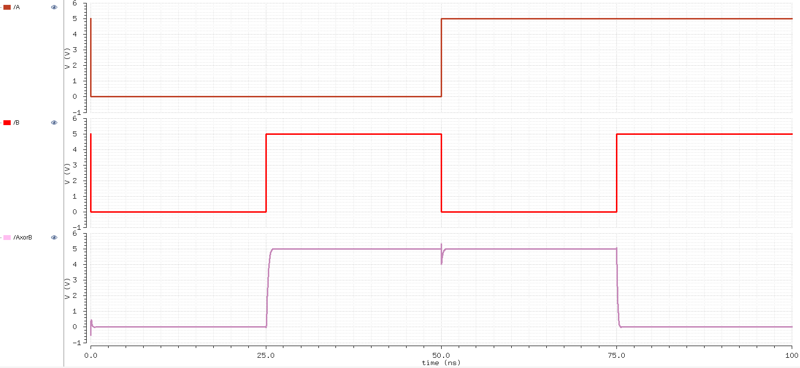
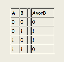
I simulated the XOR gate to ensure that the output matched the truth table of a 2-input XOR gate.

The output was a 1 when the inputs differed, and a 0 when the inputs were the same.


Spectre Simulation Result Truth Table
http://cmosedu.com/jbaker/courses/ee421L/f17/students/baej8/proj/images/xor_sim.PNG http://cmosedu.com/jbaker/courses/ee421L/f17/students/baej8/proj/images/xor_truth.PNG


    Designing a 2-input XNOR gate


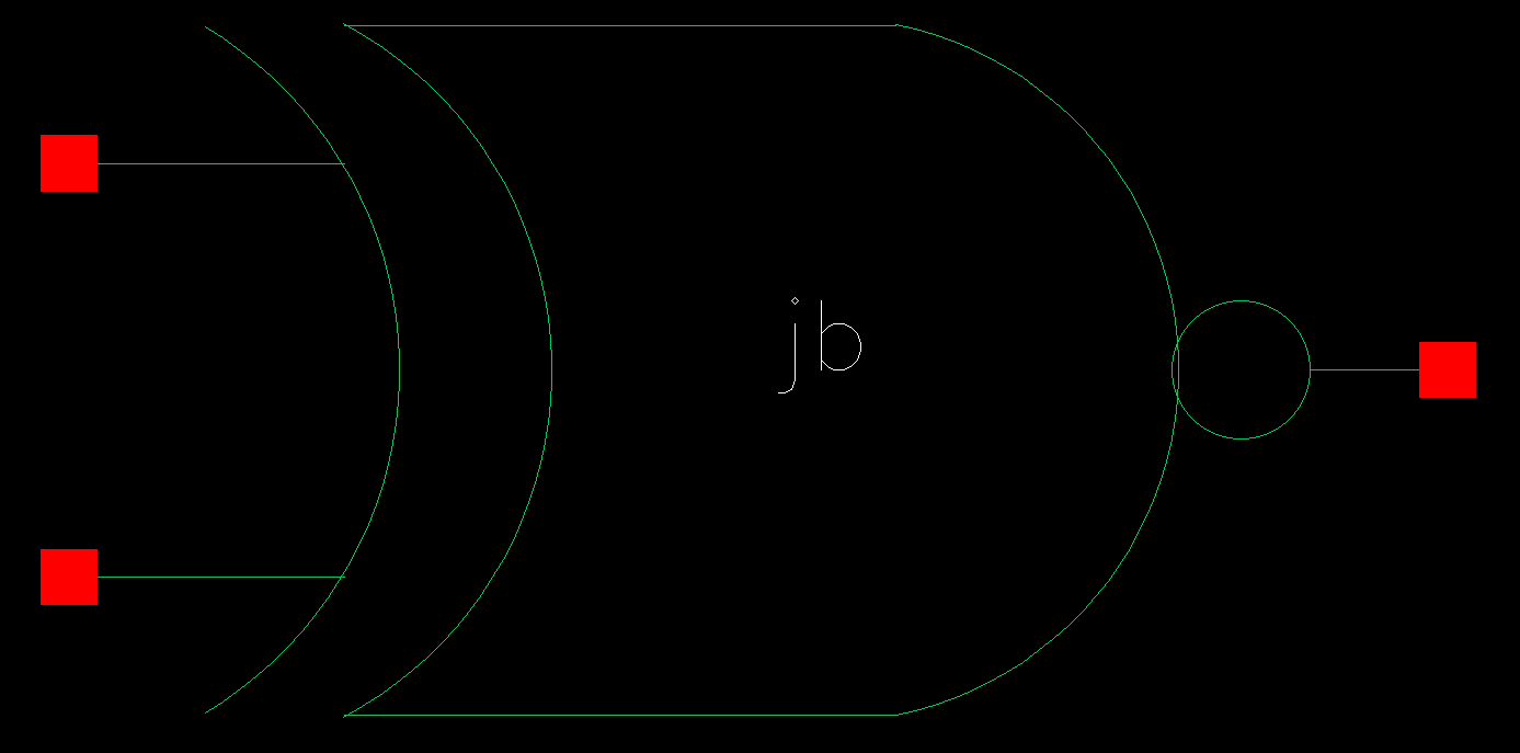
Likwise, I created a schematic and a symbol for the commonly used XNOR gate by attaching an inverter to the output of the XOR gate. Below are the images of the XNOR gate.
     
Schematic Symbol
http://cmosedu.com/jbaker/courses/ee421L/f17/students/baej8/proj/images/xnor_schematic.PNG http://cmosedu.com/jbaker/courses/ee421L/f17/students/baej8/proj/images/xnor_symbol.PNG
   

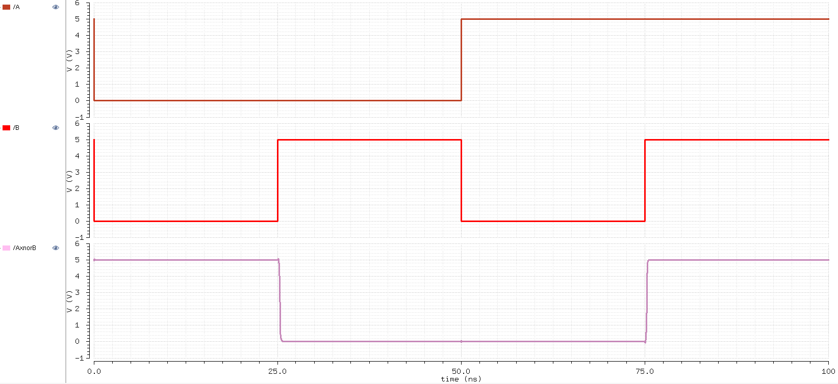
I simulated the XNOR gate to ensure that the output matched the truth table of a 2-input XNOR gate.

The output reflected the inverted signal of a XOR gate; the output was a 1 when the inputs were the same, and a 0 when the inputs were different.


Spectre Simulation Result Truth Table
http://cmosedu.com/jbaker/courses/ee421L/f17/students/baej8/proj/images/xnor_sim.PNG http://cmosedu.com/jbaker/courses/ee421L/f17/students/baej8/proj/images/xnor_truth.PNG
     
    Designing a Buffer


To drive loads off-chip, 2 inverters with increasing sizes were used to amplify the output signal before connecting to a pad.
Furthermore, 2 diodes were used to implement ESD protection so that when the output signal goes above vdd! or below gnd!, the diodes turn on and sucks off the excess charge.
Below is the schematic and a symbol for the buffer design.

     
Schematic Symbol
http://cmosedu.com/jbaker/courses/ee421L/f17/students/baej8/proj/images2/buffer_schematic.PNG
http://cmosedu.com/jbaker/courses/ee421L/f17/students/baej8/proj/images2/buffer_symbol.PNG


    Even Parity Checker Schematic

   
I chose XOR gates to check if the 8 data bits were equal to an even number of 1's. If the 2 inputs of a single XOR gate is even (00 or 11), then the output is a 0.
Using this concept, the XOR gates were cascaded together so that the output of the last XOR was a 0 if the data bits were even, and a 1 when the data bits were odd.
To check the parity bit, a XNOR gate was used to see if the total number of input bits were equal to an even number of 1's.
If the data bits were even (0) and the parity bit was 1, then the output was 1 because the total number of inputs bits was odd.
Lastly, I used a digital output pad to ensure the ouput signal was buffered to drive loads off chip.
   
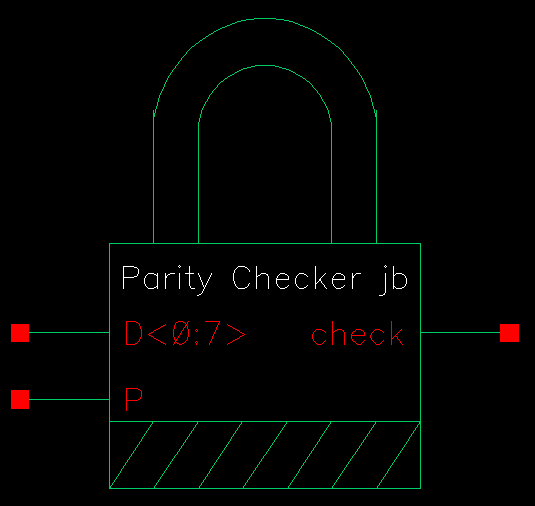
Below is the full schematic of my even parity checker circuit with a symbol representing a lock because a lock opens only if the input is valid.  
     
Schematic Symbol
http://cmosedu.com/jbaker/courses/ee421L/f17/students/baej8/proj/images/schematic.PNG http://cmosedu.com/jbaker/courses/ee421L/f17/students/baej8/proj/images/symbol.PNG
       

    Even Parity Checker Simulations


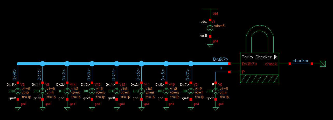
I simulated the parity checker from above to verify that the parity checker functioned as expected.

I chose to vary only 3 input bits (D<0:1> and P) because the concept of XORing 2 input bits was the same throughout.

     
Simulation Schematic
http://cmosedu.com/jbaker/courses/ee421L/f17/students/baej8/proj/images/sim_schematic.PNG
   

* The veritcal lines correspond to different inputs that were tested and can be referenced in the table below


Spectre Simulation Result
http://cmosedu.com/jbaker/courses/ee421L/f17/students/baej8/proj/images/sim_schematic_wave.PNG
     
Simulation Reference Table
P (parity bit) D<0:7> check
V1 0 0 0 1 1 1 1 1 1 1
V2 1 0 0 1 1 1 1 1 1 0
V3 0 0 1 1 1 1 1 1 1 0
V4 1 0 1 1 1 1 1 1 1 1
V5 0 1 0 1 1 1 1 1 1 0
V6 1 1 0 1 1 1 1 1 1 1
V7 0 1 1 1 1 1 1 1 1 1
V8 1 1 1 1 1 1 1 1 1 0
     
The Layout

*Click on the images to enlarge the layout and extracted views

   
   2-input XOR gate
     
Below are the layout and the extracted views of the 2-input XOR gate.
I used standard cell frames that snapped together end-to-end so that I can easily put together the cascading XOR gates for the final parity checker layout.
    

LayoutDRC successful ExtractedLVS successful
http://cmosedu.com/jbaker/courses/ee421L/f17/students/baej8/proj/images2/xor_layout.PNGhttp://cmosedu.com/jbaker/courses/ee421L/f17/students/baej8/proj/images2/xor_drc.PNGhttp://cmosedu.com/jbaker/courses/ee421L/f17/students/baej8/proj/images2/xor_extracted.PNGhttp://cmosedu.com/jbaker/courses/ee421L/f17/students/baej8/proj/images2/xor_lvs.PNG
   
   
2-input XNOR gate
     
Below are the layout and the extracted views of the 2-input XNOR gate.
     
LayoutDRC successful ExtractedLVS successful
http://cmosedu.com/jbaker/courses/ee421L/f17/students/baej8/proj/images2/xnor_layout.PNGhttp://cmosedu.com/jbaker/courses/ee421L/f17/students/baej8/proj/images2/xnor_drc.PNGhttp://cmosedu.com/jbaker/courses/ee421L/f17/students/baej8/proj/images2/xnor_extracted.PNGhttp://cmosedu.com/jbaker/courses/ee421L/f17/students/baej8/proj/images2/xnor_lvs.PNG
     
   
Buffer Layout
   
Below are the layout and the extracted views of the buffer.
The close-up views focus on the inverters for gain, and the diodes for ESD protection.
     
LayoutClose-up view of LayoutDRC successful 
http://cmosedu.com/jbaker/courses/ee421L/f17/students/baej8/proj/images2/buffer_layout.PNGhttp://cmosedu.com/jbaker/courses/ee421L/f17/students/baej8/proj/images2/buffer_layout_closeup.PNGhttp://cmosedu.com/jbaker/courses/ee421L/f17/students/baej8/proj/images2/buffer_drc.PNG
ExtractedClose-up view of ExtractedLVS successful
http://cmosedu.com/jbaker/courses/ee421L/f17/students/baej8/proj/images2/buffer_extracted.PNGhttp://cmosedu.com/jbaker/courses/ee421L/f17/students/baej8/proj/images2/buffer_extracted_closeup.PNGhttp://cmosedu.com/jbaker/courses/ee421L/f17/students/baej8/proj/images2/buffer_lvs.PNG
       
   
Even Parity Checker Layout
     
Below are the layout and the extracted views of the parity checker.
The close-up views focus on the logic gates of the parity checker.
The XNOR gate is on the botton right of the close-up view, and all the global signals (vdd! and gnd!) were tied together.
   
LayoutClose-up view of LayoutDRC successful
http://cmosedu.com/jbaker/courses/ee421L/f17/students/baej8/proj/images2/paritychecker_layout.PNGhttp://cmosedu.com/jbaker/courses/ee421L/f17/students/baej8/proj/images2/paritychecker_layout_closeup.PNGhttp://cmosedu.com/jbaker/courses/ee421L/f17/students/baej8/proj/images2/paritychecker_drc.PNG
ExtractedClose-up view of ExtractedLVS successful
http://cmosedu.com/jbaker/courses/ee421L/f17/students/baej8/proj/images2/paritychecker_extracted.PNGhttp://cmosedu.com/jbaker/courses/ee421L/f17/students/baej8/proj/images2/paritychecker_extracted_closeup.PNGhttp://cmosedu.com/jbaker/courses/ee421L/f17/students/baej8/proj/images2/paritychecker_lvs.PNG
     
   
Even Parity Checker Extracted Simulations


I simulated the parity checker layout from above to verify that the parity checker functioned as expected.

This time around, I varied all the input bits to ensure the workings of all the gates.

The simulation netlist shows proof of simulating the extracted portion of the design.


* The veritcal lines correspond to different inputs that were tested and can be referenced in the table below


Spectre Extracted Simulation ResultSimulation Netlist
http://cmosedu.com/jbaker/courses/ee421L/f17/students/baej8/proj/images2/sim_extracted.PNGhttp://cmosedu.com/jbaker/courses/ee421L/f17/students/baej8/proj/images2/sim_netlist.PNG
       
Extracted Simulation Reference Table
P (parity bit) D<0:7> check
V1 0 0 0 1 1 0 1 0 1 1
V2 1 0 0 0 1 1 1 0 0 1
V3 0 0 1 1 0 0 1 1 1 0
V4 1 0 1 0 0 1 1 1 0 0
V5 0 1 0 1 1 0 0 0 1 1
V6 1 1 0 0 1 1 0 0 0 1
V7 0 1 1 1 0 0 0 1 1 0
V8 1 1 1 0 0 1 0 1 0 0
   
The design worked as expected as seen in the simulations of both the schematic and extracted portions.
     
Final design directory: proj_jb.zip
     

Return to Junho's Labs

Return to EE421L Labs