Lab 02 -
EE 421L
Authored
by Junho Bae
baej8@unlv.nevada.edu
September
13, 2017
Pre-lab
work
After
downloading and uploading lab2.zip to the design directory, I unzipped
the file, and added the necessary statement to my cds.lib (DEFINE lab2 $HOME/CMOSedu/lab2).
I started Cadence and opened the schematic view of the cell
sim_Ideal_ADC_DAC.
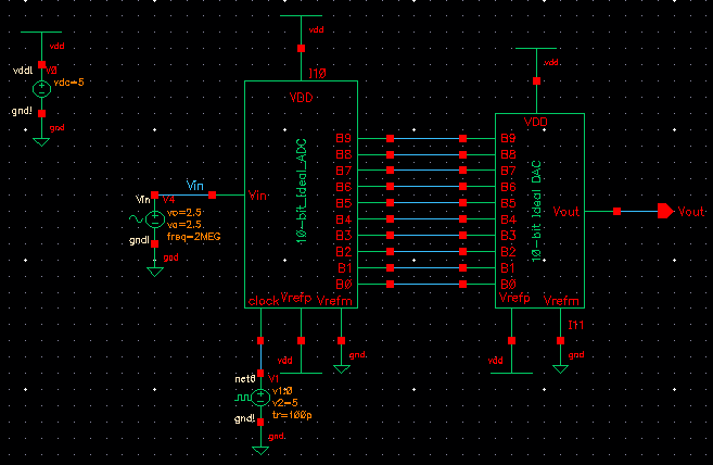
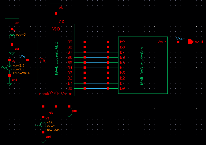
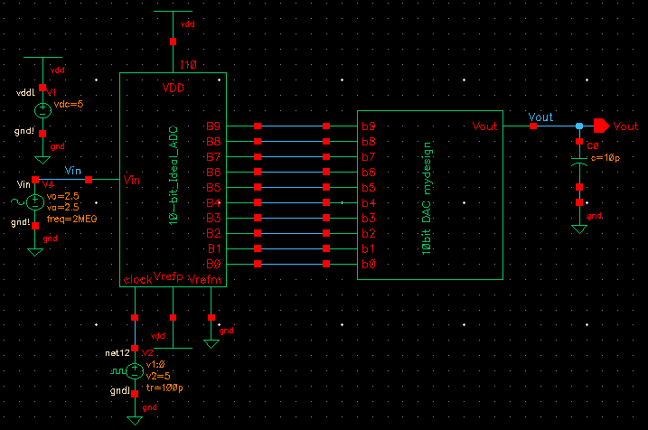
Below is the schematic of the ideal 10-bit ADC and DAC.

Launching the ADE, I ran the simulation to see the input voltage of the
ADC, and the ouput voltage of the DAC.
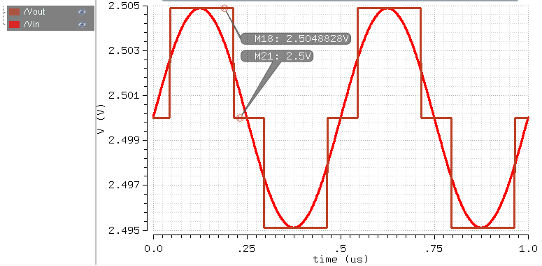
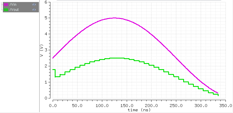
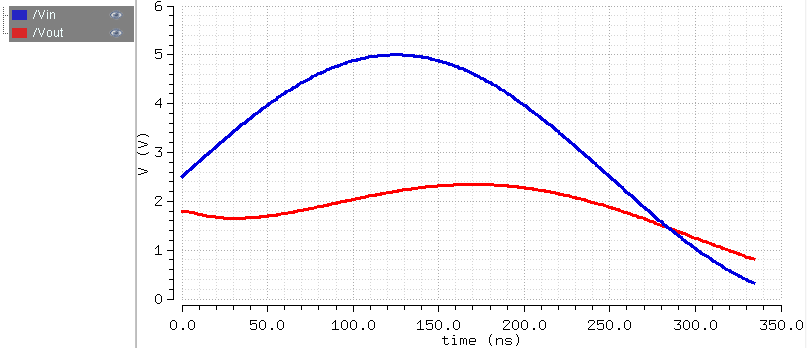
Below is the simulation result of the previous schematic.

The
analog signal represented by the blue line is the input signal that is
being inputted into the 10-bit ADC which is then converted to a digital
signal that can be represented through 10 bits. The 10 bits are then
used as the input of the 10-bit DAC which converts the 10-bit digital
signal to an analog signal represent by the green line.
The
ideal 10-bit DAC is limited by a reference voltage (Vdd) because you
cannot rebuild a signal with less power than the signal is suppose to
carry. The simulation below shows a modified input sine wave (4V,
offset of 3V) that
surpasses the the reference voltage which clipped the reconstructed
analog signal to 5V.
 |
 |
The
LSB represents the smallest voltage level an ADC can convert to 1 bit.
Likewise, it is the smallest voltage that a DAC can represent through 1
bit.

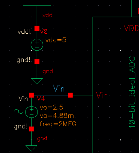
The simulation below shows a 4.88mV input signal which corresponds to 1
step of the output signal.
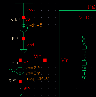
If the signal is lower than 4.88mV, the ADC cannot convert the voltage
to a digital signal because the LSB is 4.88mV.
The simulation below shows a 2mV input signal which cannot be converted
as seen by the output signal.
Lab
Work
Designing
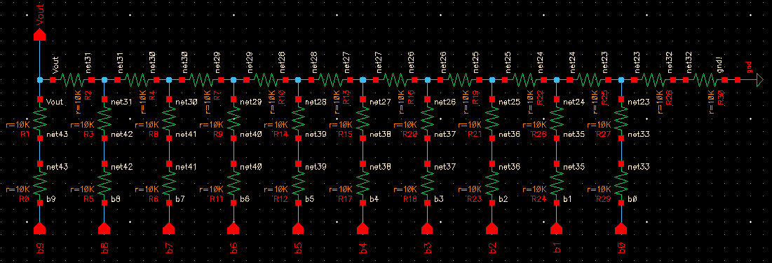
a 10-bit DAC using n-well resistors
The
first part of the lab involved designing my own 10 bit DAC using a
combination of 10K resistors.
After I completed the design and drafted my schematic to replicate a
10-DAC, I turned it into a symbol.

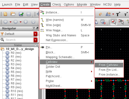
By going to create -> cellview -> cellcreate, I was able
to create a symbol view of my design.

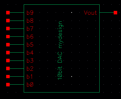
Below
is the symbol view of my 10-bit DAC design. Similar to the footprint as
the Ideal_10-bit_DAC, I removed the unecessary components such as
Vrefp, VDD, and Vrefm.

Total Output
Resistance of DAC
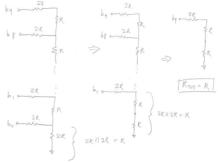
By
first combining the resistors in parallel of the least significant bit,
I was able to see that the combination resulted in just R. This created
the very same circuit before of 2R in parallel with 2R. By continuing
this process, I calculated the total output resistance of the DAC to be
R.

Delay, driving a
load
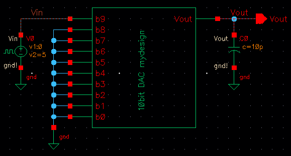
In order to generate a delay using a DAC, all inputs except b9 were
grounded (b[9:0]).
b9 was connected to a 0 to 5 voltage pulse source, and a 10pF capacitor
load was added.
The
expected output was a fourth of the input voltage due to the voltage
divider, and the time delay of 50% of the output voltage.

Below is the simulation of the output voltage.
By using 0.7RC to predict the time delay, it should take around
0.7*10k*10pF = 70ns for the output voltage to reach 1.25V.
As predicted, the actual time to reach 1.25 voltages was 72ns which is
close to 70ns.

Simulations to
verify my design function correctly
To
verify that my design was working as expected, I copied the schematic
cell view of the original simulation (sim_Ideal_ADC_DAC) to a new cell
(sim2_Ideal_ADC_DAC) and replaced the ideal DAC with the DAC I
designed.
The simulation of the designed DAC matches the orginal simulation;
therefore, works as expected.
 |
 |
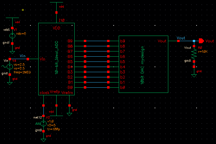
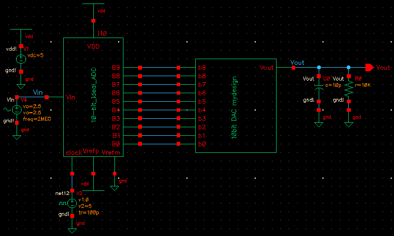
Driving a resisitive load
The
resisitive load creates an additional voltage divider which overall
reduces the output voltage based on the value of the resistor. In the
simulation below I used a 10k resistor which reduced the output voltage
by half.
Driving a capacitive load
The
capacitor creates a low pass filter which cleans the edges of the DAC
output. However, the capacitive load creates a phase shift depending on
the value of the capacitor. Below is the simulation results of the
smoothened output signal.
Driving a RC load
Similar
to the previous two simulations, the resistor and capacitor replicates
the effects of both components. The output voltage is reduced due to
the voltage divider, the signal is filtered, and there is a
phase
shift as seen in the simulation below.
Explain what happens if
the DAC drives a 10k load.
If
the DAC drives a 10K
resistor, the output voltage drops to half of the input voltage due to
the additonal voltage divider being created.
Discuss what happens if
the resistance of the switches isn't small compared to R.
Using
switches with resistances that are not much less than R results in the
output voltage decreasing as the resistor of the switch in series with
2R limits more current.
Backing up my files

Return
to Junho's Labs
Return
to EE421L Labs
