EE 421L: Digital Integrated Circuit Design Lab -
Project
Due Date: 11/15/2017
Link to directory:
<< proj_fa17.zip>>
Design an even parity
checking circuit having a 9-bit input word, 8-bits of data and 1-bit parity,
that outputs a 1 (0), when the even parity check
is valid (invalid).
Inputs: D<0:7>
and P
Outputs: check
The output of the
design should be buffered before connecting to a pad.
Generating the Even
Parity Bit
When generating an
even parity bit for a given word, the output should follow the following table.
|
Input D<0:7> |
Output |
|
If total number of
“1s” is even |
0 |
|
If total number of
“1s” is odd |
1 |
To generate the
parity bit for the 8-bit word, one can use a total of seven 2-input XOR gates
in the following topology,
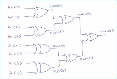
Figure: sketch of schematic
The corresponding
schematic and symbol in Virtuoso are shown below.

Figure: parity bit
generator schematic

Figure: parity bit
generator symbol
Checking the Parity
Bit
If the parity bit that
was generated agrees with input (P), then the circuit should output a “1” and
if they’re different then the output become a “0”. This logic can be
implemented a single 2-input XNOR gate.
The previously
designed XOR gate from lab 6 was modified to create an XNOR gate (shown below).

Figure: XNOR
schematic

Figure: XNOR symbol
Using this XNOR gate
the parity checker was assembled with the following schematic.

Figure: parity
checker schematic

Figure: parity
checker symbol
Buffer Circuit
Before connecting the
output (check) to a pad the output needs to go through a buffer so that there
are not large delays due to capacitances on the bonding pad. The buffer used is
shown below along with its symbol.
|
Figure: Buffer
circuit schematic |
Figure 1: Buffer circuit symbol |


Simulating Delay
The schematic used to
simulate the delay of the even parity checker with the buffer is shown below.
In the schematic
below, all input data bits are grounded except for D<0>. The parity bit generated from the input data will
effectively be the same as D<0>.
As a result, if D<0> matches P then the parity check will output
high. If they differ then the parity check will output low.
As shown in the
simulation results, the delay of the output with the buffer with a load of a
1pF capacitor is 2.115 ns and the transition from high-to-low or low-to-high is
steep.

Figure: Simulating
the delay of the Parity checker and Buffer

Figure: simulation
results of parity checker and the buffer
Additional Simulation
A second simulation
is shown with various inputs being fed to the Parity Checker.
The results of the
simulation show the Parity Checker functioning as expected.

Figure: schematic
for simulating Parity Checker

Figure: simulation
results of the parity checker
Part II: Layouts
Parity Generator
layout:

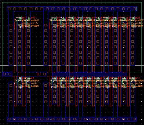
Figure: even parity
bit generator layout

Figure: even parity
bit generator extracted view
DRC and LVS results:

Figure: DRC results
for the parity generator

Figure: LVS results
for parity generator
XNOR gate Layout
|
Figure: XNOR
layout |
Figure: XNOR
extracted |


DRC and LVS:
|
Figure: DRC
results for XNOR gate |
|
Figure: LVS results
for XNOR gate |


Parity Checker Layout:

Figure: Parity checker
layout

Figure: Parity
checker extracted
DRC and LVS results:

Figure: DRC results
for Parity checker

Figure: LVS results
for Parity checker
Buffer layout
|
Figure: Buffer
layout |
Figure: Buffer
extracted |

DRC and LVS results:

Figure: DRC results
for the buffer

Figure: LVS results
for the buffer
Simulating the
Extracted Schematics:

Figure: schematic for simulating the extracted schematics

Figure: simulation
results
Return to Students
Return to Labs