EE 421L: Digital Integrated Circuit Design Lab - Lab
6
Due Date: 10/25/2017
In this lab, we
design two-input XOR and NAND gates then use them to design a Full Adder.
Frame for Layouts:
For the layouts in
this lab, a frame was laid out so that all the gates would fit together when
laid out side to side. Connections to VDD were placed at the top of the frame
while connections to GND were placed towards the bottom. The height of the
frame was made several times larger to accompany multiple metal wires running
horizontal between the NMOS and the PMOS.
For the layouts in
this lab, metal_2 was designated for horizontal wiring and metal_1 was
designated for vertical wiring. This was done to avoid crossing wires and to
keep the layout as organized as possible for complicated layouts.
**All MOSFETs used in
this lab are sized: W/L = 6u/600n**

Figure 1: Frame layout
NAND Gate:
A two-input NAND gate
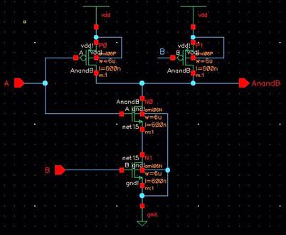
was used for this lab. The schematic for the NAND gate and its corresponding
symbol is shown below. For the layout of the NAND gate, the standard cell frame
from above was used as a template. The pins for the layout were placed on
Metal_1.
|
Figure 2: NAND gate schematic |
Figure 3: NAND gate layout |
Figure 4: NAND gate extracted |
|
Figure 5: NAND gate symbol |
NAND DRC and LVS
results:
|
Figure 6: DRC results for NAND gate |
Figure 7: LVS results for NAND gate |
NAND Gate Simulation:
The extracted layout
from above was simulated with the schematic shown below. The simulation results
show that the designed NAND gate follows its truth table correctly.
**Regarding glitches,
The plot also shows
that during transitions in the input voltages, the output of the gate goes
through short glitches due to the fact that there is a period where the inputs
are neither on or off but somewhere in between.
|
Figure 8: NAND gate simulation
schematic |
Figure 9: NAND gate simulation
results |
XOR Gate:
Next, a two-input XOR
gate was designed. The schematic for the XOR gate is shown below as well as its
symbol.
The XOR gate layout consists
of the two inverters placed on both ends with the other eight MOSFETS in the
center. The eight MOSFETs in the center were laid out end to end so that the
layout size would be kept small. Due to the smaller space, allocating Metal_1
for vertical wiring and Metal_2 for horizontal wiring helped keep the layout
manageable. The pins in this layout were all placed on Metal_1.
|
Figure 10: XOR schematic |
Figure 11: XOR symbol |
|
Figure 12: XOR layout |
Figure 13: XOR extracted |
DRC and LVS results:
|
Figure 14: XOR DRC results |
Figure 15: XOR LVS results |
XOR Gate Simulation:
The extracted layout
was simulate using the schematic shown below. From the simulation results, we
see that the circuit performed as expected.
|
Figure 16: XOR simulation schematic |
Figure 17: XOR simulation results |
Full Adder Design:
The Full Adder was
then designed using the gates from above. The schematic and corresponding
symbol is shown below.
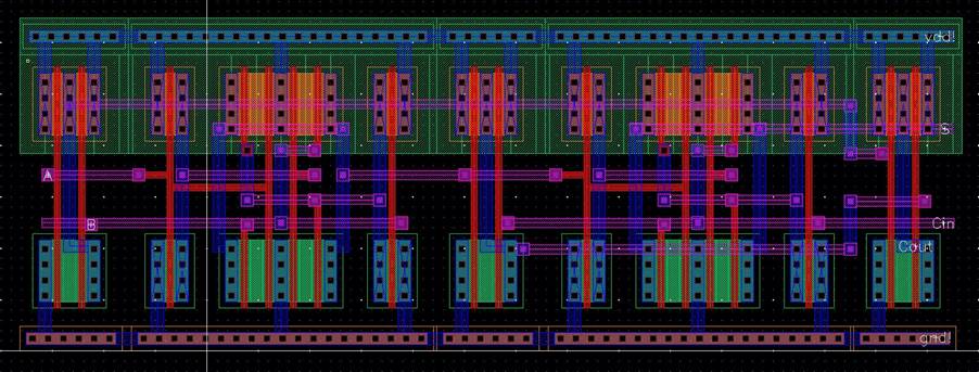
For the layout of the
full adder, the layouts for the XOR and NAND gates were instantiated into the
layout window and placed end-to-end. Since the NAND gate had lots of empty
space in between the NMOS and PMOS, the m1_poly connections were moved up or
down depending on what was convenient for the layout. The pins in this layout
were placed on Metal_1 and Metal_2.
|
Figure 18: Full Adder schematic |
Figure 19: Full Adder symbol |
|
Figure 20: Full Adder Layout |
|
|
Figure 21: Full Adder extracted |
|
DRC and LVS results:
|
Figure 22: Full Adder DRC results |
Figure 23: Full Adder LVS results |
Simulation of Full
Adder:
The following
schematic was used for the simulation of the full adder. The Transient Response
shows that the extracted layout performs as expected.
|
Figure 24: Full Adder simulation
schematic |
|
Figure 25: Full Adder simulation
results |
Return to Students
Return to Labs


