EE 421L: Digital Integrated Circuit Design Lab - Lab
5
Due Date: 10/11/2017
Link to directory:
<<lab5_ga.zip>>
In this lab, we layout
two inverter designs and then simulate them while varying a capacitive load to
compare their performances.
Design
The first design uses
a PMOS with a width/length of 12u/0.6u and an NMOS with a width/length of
6u/0.6u. The second design uses four branches of the first design.
Schematics and
symbols of the inverters are shown below:
|
Figure 1: schematic of inverter 12/6 |
Figure 2: symbol of inverter 12/6 |
|
Figure 3: schematic of inverter
48/24 |
Figure 4: symbol of inverter 48/24 |


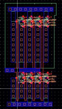
Layout
The layouts of both
inverters are shown below. The layout of the second inverter consisted of
placing multiple MOSFETS side by side with each one sharing at least one metal
terminal with another to reduce layout area. Both layouts had 4 pins consisting
of A, Ai, vdd!, and gnd!.
|
Figure 5: Layout view of 12/6
inverter |
Figure 6: Extracted view of 12/6
inverter |
Figure 7: Layout view of 48/24
inverter |
Figure 8: Extracted view of 48/24 inverter |


DRC and LVS results:
|
Figure 9: DRC results for 12u/6u
inverter layout |
Figure 10: LVS results for 12u/6u
inverter |
|
Figure 11: DRC results for 48u/24u
inverter layout |
Figure 12: LVS results for 48u/24u
inverter |


Simulation:
A parametric analysis
was performed on the following circuit where the value of the capacitive load
was changed from 100 fF to 100 pF with one step per
decade.
In the simulations,
we observe that as the capacitive load increases, the inverter takes a longer
time to react to the step response. Comparing the two inverter designs, we see
that the 48/24 inverter design performs better than the 12/6 inverter. This is
due to the 48/24 inverter having an additional 3 branches that allow the
capacitor to charge and discharge more quickly.
**UltraSim
is a Cadence simulator for simulating larger circuits with the cost of
decreased accuracy. The UltraSim simulations below show
similar results to those using Spectre. This is due
to the fact that the circuit wasn’t large enough to warrant any difference.
|
Figure 13: simulation schematic for
12/6 inverter |
Figure 14: Spectre
simulation results |
|
|
Figure 15: UltraSim
simulation results |
|
Figure 16: simulation schematic for
48/24 inverter |
Figure 17: Spectre
simulation results |
|
|
Figure 18: UltraSim
simulation results |


Return to Students
Return to Labs