EE 421L: Digital Integrated Circuit Design Lab - Lab
4
Due Date: 9/27/2017
In this lab we
practice laying out NMOS and PMOS transistors with probing pads attached to
each terminal. The transistors are then characterized by generating Current vs.
Voltage curves.
Making a Probe Pad:
The probe pads for
each terminal in the MOSFETs are going to be smaller than a typical bonding pad.
To design the probe pad, one should consult the design rules first. According
to the design rules, the minimum probe passivation opening (minimum
length/width) allowed is 20 micrometers. In addition to this, the amount of pad
metal that overlaps the passivation opening should be at least 6 micrometers.
Using these design rules, the probe pad can be laid out.
|
Dimensions of Probe Pad: Glass Layer: L=W=22.5 um Metal3: L=W= 36 um |
|
|
Figure 1: Probe Pad Schematic
Figure 2: Probe Pad Symbol |
Figure 3: Probe Pad Layout |


NMOS and PMOS
schematic and symbols:
Before laying out the
transistors, a corresponding schematic and symbol is generated. The NMOS
transistor’s length will be 600 nanometers and its width is 6 micrometers. The
PMOS will have the same length as the NMOS but will have a width of 12
micrometers.
In a schematic
window, the four-terminal MOSFET symbol is instantiated. Then pins and the probe
pads are placed on each of MOSFET’s four terminals. Once the schematic is
finished, a symbol is created which will then be used to create IV curves later
in the lab.
|
Figure 4: NMOS schematic |
Figure 5: NMOS symbol |
|
Figure 6: PMOS schematic |
Figure 7: PMOS symbol |


Layout
For the layout, the
probe pad created in the steps above was instantiated into the layout view.
Once again, the design rules have to be considered when laying out multiple
pads. According to the rules, the minimum distance between two unrelated Metal3
pads is 30 micrometers. As a result, the probe pads were separated from one
another by 30 um.
The MOSFET was then
instantiated in a way that allowed metal wires to be routed easily from the
pads to the terminals. In addition to the MOSFET cells from the NCSU library,
the following had to be added to the transistors to complete their design: For the NMOS, a p-tap cell was instantiated
in order to provide a connection to the body (p-substrate) of the NMOS. For the
PMOS, an n-tap cell was instantiated next to the PMOS’s n-well so that a body connection
could be made.
To minimize the
resistance of the connections of the MOSFET to the probe pads, the routing
wires were made considerably wide and multiple vias were instantiated in
between the metal layers. The final layout for both NMOS and PMOS transistors
is shown below,
|
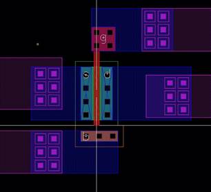
Figure 8: NMOS layout zoomed out |
Figure 9: NMOS layout zoomed in |
|
Figure 10: PMOS layout zoomed out |
Figure 11: PMOS layout zoomed in |


DRC and LVS:
The results after performing DRC and LVS are
shown below for both layouts,
|
DRC |
LVS |
|
Figure 12: DRC results for NMOS
layout |
Figure 13: LVS for NMOS |
|
Figure 14: DRC results for PMOS
layout |
Figure 15: LVS for PMOS |


Simulations:
The following IV
curves where generated by simulating the layout of the MOSFETS.
|
Schematic |
IV Curves |
|
Figure 16: NMOS simulation schematic |
Figure 17: Id vs. Vgs curve with Vds = 100mV |
|
|
Figure 18: Id vs. Vds
with Vgs going from 0 to 5 volts in 1 volt steps. |
|
Figure 19: PMOS simulation schematic |
Figure 20: Id vs. Vsg
curve with Vsd = 100 mV |
|
|
Figure 21: Id vs. Vsd with Vsg going from 0 to 5 volts in 1 volt steps. |


Return to Students
Return to Labs