Lab
7 - EE 421L
Authored
by
Charlie Torres-Garcia
torresga@unlv.nevada.edu
11/15/2016
Using
buses and arrays in the design of word inverters, muxes, and high-speed adders
Pre-lab
work
- Back-up
all of your work from the lab and the course.
- ALL
work has been updated to Google Drive as previous labs.
- Go
through Tutorial
5.
Tutorial 5 goes over Ring Oscillator: Design/Layout/ and simulation.
Schematic:

Layout:

DRC: LVS:


____________________________________________________________________________________________________________________________________________
Lab
6 covers the design, layout, and simulation of 4-Bit inverter, {8-bit
input/output array of: NAND, NOR, AND, inverter, and OR gates}, a 2-to-1
DEMUX/MUX, a 8-bit
wide word 2-to-1 DEMUX/MUX, a full-adder, and a 8-bit full-adder.
4-Bit
Inverter:
Schematic:

Symbol:

Layout: Extraction:


Sim:


Capacitance loads does influence the delay, rise and fall times. High cap. causes delay in fall and rise significantly. Low cap. has better fall and rise as seen in green. And no cap. is ideal fall and rise seen in red.
Create
schematics and symbols for an 8-bit input/output array of: NAND, NOR, AND, inverter, and OR gates.
Provide
a few simulation examples using these gates.
8-Bit
NAND:
Previously made NAND (Schematic/Symbol) in lab. Using instance and concise method of this gate, we get:
Schematic:

Symbol:

8-Bit
NOR:
Previously made NOR (Schematic/Symbol) in lab. Using instance and concise method of this gate, we get:
Schematic:

Symbol:

8-Bit
AND:
Previously made AND (Schematic/Symbol) in lab. Using instance and concise method of this gate, we get:
Schematic:

Symbol:

8-Bit
INVERTER:
Previously made INVERTER (Schematic/Symbol) in lab. Using instance and concise method of this gate, we get:
Schematic:

Symbol:

8-Bit
OR:
Previously made OR (Schematic/Symbol) in lab. Using instance and concise method of this gate, we get:
Schematic:

Symbol:

Provide
a few simulation examples using these gates.
Here we create a new Schematic with all the 8-Bit Gates to sim the logic.
Schematic to sim all logic:


Next
examine the following schematic.
T2-to-1
DEMUX/MUX
Simulate the operation of this circuit using Spectre and explain how it works.
Make
sure to show, using simulations, how the circuit can be used for both multiplexing and de-multiplexing.
Schematic:
Symbol:


Multiplexing
SIM:


De-Multiplexing
SIM:


Create
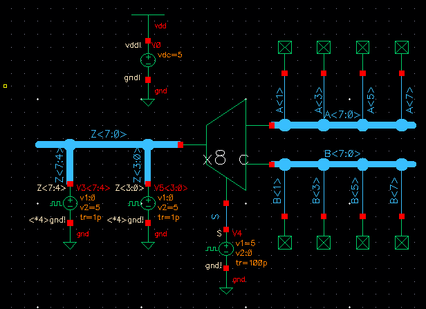
an 8-bit wide word 2-to-1 DEMUX/MUX schematic and symbol.
8-bit
wide word 2-to-1 DEMUX/MUX:
Schematic:

Symbol:

8-Bit
Multiplexing SIM:


8-Bit
De-Multiplexing SIM:


Finally, draft the schematic of the full-adder seen in Fig. 12.20 using 6u/0.6u devices (both PMOS and NMOS).
Create an adder symbol for this circuit (see the symbol used in lab6).
Full-Adder:
Schematic:

Symbol:

Layout: Extraction:


DRC: LVS:


Use this symbol to draft an 8-bit adder schematic and symbol.
8-Bit Full-Adder:
Schematic:

Symbol:

Layout: Extraction:


DRC:

Return
To EE 421L Labs


