Lab 5 - EE 421L
Authored
by Charlie Torres-Garcia
torresga@unlv.nevada.edu
10/4/2016
Digital Integrated Circuit Design -
Design, layout, and simulation of a CMOS inverter
Pre-lab:
Files are backed up in (Drive and Laptop)
Go through Tutorial 3 seen here.
The first step in Making the inverter is to create a schematic for the CMOS inverter using NMOS and PMOS.
Picking NMOS 6u/600n and PMOS 12u/600n we get the following:
Schematic: Re-Drawing the symbol to make it look like an inverter:


The next part is to create the layout and extraction in the same cell view where we made the schematic/symbol.
Adding the following cells (nmos, pmos, ntap, ptap, and m1_poly) we create he layout:
Layout: (connecting NMOS to gnd! and PMOS tovdd!) Extraction:


We DRC and LVS to make sure our layout is designed correct.
DRC: LVS:


Now we save and we create a new schematic to sim the new inverter.
We instance the inverter and set up the the sim to get:
Schematic: Sim:


_________________________________________________________________________________________________________________________________________________________
Post-lab:
Draft schematics, layouts, and symbols for two inverters having sizes of:
12u/6u (= width of the PMOS / width of the NMOS with both devices having minimum lengths of 0.6u)
48u/24u where the devices use a multiplier, M = 4
12u/6u INVERTER:
The 12u/6u was created during Tutorial 3 in the pre-lab. (SEEN above).
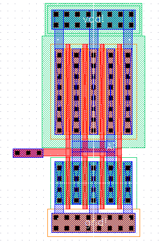
48u/24u INVERTER (M=4):
Following the same steps as the 12u/6u inverter (Schematic/Symbol/Layout/Extraction/DRC/LVS) we get the following:
Schematic: Symbol:


Layout: Extraction:

DRC: LVS:


Using SPICE simulate the operation of both of your inverters showing each driving a 100 fF, 1 pF, 10 pF, and 100 pF capacitive load.
We simulate both created inverters with the following loads.
Pointing at the MOSFET models in Setup. and (Simulator/Directory/Host and select UltraSim)
Also for all the load simulations I used transient @ 30n and the following VPULSE settings for all the sims ==>

12u/6u INVERTER:
Schematic:

100 fF: UltraSim yields the same exact sim:


1p :


10p:


100p:


48u/24u INVERTER:
Schematic:

100 fF


1p:


10p:


100p:


LAB5.ZIP
Return To EE 421L Labs