Lab 4 - EE 421L 

Authored by Charlie Torres-Garcia 

torresga@unlv.nevada.edu


9/27/2016


EE 421L Digital Integrated Circuit Design
IV characteristics and layout of NMOS and PMOS devices in ON's C5 process


Pre-lab:

Back-up all of your work from the lab and the course. 

Going through Tutorial 2

In Tutorial 2 we make an 6u/600n NMOS and a 12u/600n PMOS layout.


Creating NMOS:

First we create a schematic that looks like the schematic seen below with Pins (InandOut) with nmos4 (Making sure the Body is connected to gnd or making a pin labeled B) :
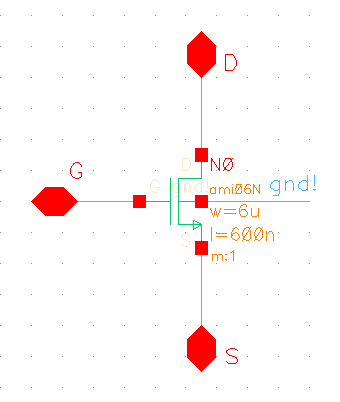

From this schematic we can output a symbol. Deleting everything from the symbol except the pins, we can create our own symbol seen below:


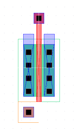
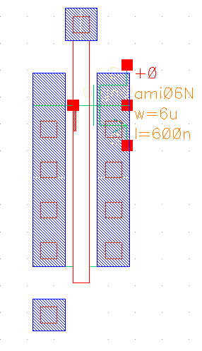
Now we are ready to do a layout view of the NMOS. Choosing the right components and libraries we create the NMOS to look like this and extract it:
Layout:                                                                               Extraction:


The final step is to DRC and LVS our NMOS to make sure it is working properly.

(We can see that DRC was completed with zero errors and LVS list matched):

DRC:                                                                                                       LVS:


Simulating NMOS to show IV curves.

To simulate the IV curves we use the NMOS symbol that was created in the previous steps and connected to 2 different voltage sources. (one at VGS and the second one at 0)


To simulate this NMOS we have to change the Model Library to standalone (ami06N.m), edit a variable (VGS=0), analysis and parameters in dc with a linear step of 1m, and choose our output current at node D. (Note that we have chosen pin B and a voltage source called VSB)


Having all the settings as seen below, we get the following results for our NMOS IV curves:


Creating PMOS:
Creating a PMOS is similar to creating a NMOS. Just remembering that the Body of the PMOS is connected to VDD. Following every step from above we get the following schematic, symbol, extraction, layout, and simulation.
Schematic:                                                                                        Symbol:
          

Layout:                                            Extraction:
            

Schematic (For simulating the IV curves of the PMOS):                      Results:
                      

____________________________________________________________________________________________________________________________________________________________

Post-lab:


Generate 4 schematics and simulations (see the examples in the Ch6_IC61 library, but note that for the PMOS body should be at vdd! instead of gnd!):


Simulating ID v. VDS of an NMOS:                         (VGS varying from 0 to 5 V in 1 V steps while VDS varies from 0 to 5 V in 1 mV steps)

To simulate ID vs VDS, we use the NMOS previously made:


Schematic:                                                                                                  Results:


Simulating ID v. VGS of an NMOS:                    ( VDS = 100 mV where VGS varies from 0 to 2 V in 1 mV steps)

To simulate IDvsVGS we have a parameter called VSB (0-1V, steps of 5).


Schematic:                                                                                                Results:


Simulating ID v. VSD of a PMOS:                             (VSG varying from 0 to 5 V in 1 V steps while VSD varies from 0 to 5 V in 1 mV steps)

To simulate ID vs VSD, we use the PMOS previously made:


Schematic:                                                                                                 Results:


Simulating ID v. VSG of a PMOS:                                                 (VSD = 100 mV where VSG varies from 0 to 2 V in 1 mV steps)

To simulate IDvsVSG we have a parameter called VBS (0-1V, steps of 5).


Schematic:                                                                                                   Results:


NOW....

Lay out a 6u/0.6u NMOS device and connect all 4 MOSFET terminals to probe pads.

To connect the NMOS to all MOSFET terminals with pads we create a new schematic using the symbol we have created previously and connect to previously created pads (courtesy of Dr. Baker).

Schematic:


Then we make a Symbol:


Now we are ready to create a layout with connected pads. We make sure we use the proper components and libraries and connect all pads with all the pins: G B S D and extracted.
Layout:                                                                                                   Extraction:
  

The final step is to DRC and LVS to make sure or NMOS device works properly.
DRC:                                                                                                                LVS:
   

Lay out a 12u/0.6u PMOS device and connect all 4 MOSFET terminals to probe pads.
To connect the PMOS to all MOSFET terminals with pads we create a new schematic using the symbol we have created previously and connect to previously created pads (courtesy of Dr. Baker).


Following all the previous steps for a pad connected NMOS we get the following for a PMOS:

Schematic:                                                                                             Symbol:


Layout:                                                                                                 Extraction:


DRC:                                                                                                              LVS:


Return To EE 421L Labs