PROJECT
- EE 421L Digital Integrated Circuit Design
Authored
by
Charlie Torres-Garcia
11/29/2016
Project - design a circuit that takes a serial input and detects (outputs a high logic signal called detect) the sequence 101011
The
inputs to your circuit are clk and in (Make sure that the output of your design, detect, is buffered before connecting to a pad)
A buffer will be needed for the output of the DETECT before connecting to the padframe.
BUFFER DESIGN
Schematic:
Symbol:


Simulation:

Layout: Extraction:

 DRC:
LVS:
DRC:
LVS:


The following circuit with inputs (clk and in) will be to implement our D Flip Flop (D-FF) for our design.
CLOCK
Schematic:
Symbol:

 Layout: Extraction: DRC: LVS:


Using CLOCKs/INVERTERs we implement a Edge-Triggered D-FF from Fig. 13.22 (pg.387).
Each device for the design is laid out prior, to ensure that the DETECTOR circuit DRC's and LVS's easier.
D-FF consists of CLOCK's and Inverters previously made to create a D-FF with 2 inputs (D/clk) and 2 outputs (Q/Q').
Edge-Triggered D-FF
Schematic:
Symbol:


Simulation:

We can see that Q and Q' both trigger on the rising edge of the CLOCK inputs (clk and in) Layout:
Extraction:


DRC:
LVS:


We create a 6-Bit NAND gate for our sequence
101011 to connect with the Edge-Triggered D-FF to finalize the DETECTOR circuit.
6-Bit NAND
Schematic:
Symbol:

 Simulation:
 Nand
simulation shows that we can output a nand high (1) and a nand low (0).
Nand
simulation shows that we can output a nand high (1) and a nand low (0).
Layout:
Extraction:

DRC:
LVS:


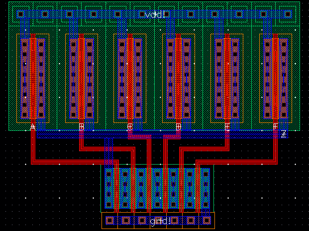
Finally the DETECTOR circuit for sequence 101011 is created using the Edge-Triggered D-FF and 6-Bit NAND circuit and layouts.
The final design of the DETECTOR has 6 D-FF's connected in series with Q (output) connected to D (input).
6-Bit NAND has 3 (Q/D) inputs, 2 (Q') inputs, and a (Q) input connected to A/B/C/D/E/F. DETECTOR
Schematic:

Symbol:
Simulation Schematic:


Simulation using 101011:
 Layout:
Extraction:
Layout:
Extraction:


 DRC:
LVS:
DRC:
LVS:


FINAL_PROJECT_ZIP
Back
To Main Directory