Lab 7 - EE 421L
nelsoz1@unlv.nevada.edu
Pre-lab:
Finish Tutorial_5 ✓
Read through
lab entirely before starting work ✓
Back-up
all previous work from Lab and the course work ✓
_________________________________________________________________________________________________________________________________
Lab
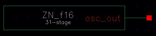
Experiment 1: 31-stage Oscillator
The
first task was doing Tutorial_5 which takes you through the steps, start to
finish of doing the 31-stage Oscillator, which is 31 inverters all connected in
series.
I set Vdd at 5V and then the output of the last inverter was fed
back into the input of the first inverter, and viola an oscillator.
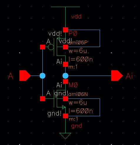
I used the schematic to create the symbol, and then I began to create the layout
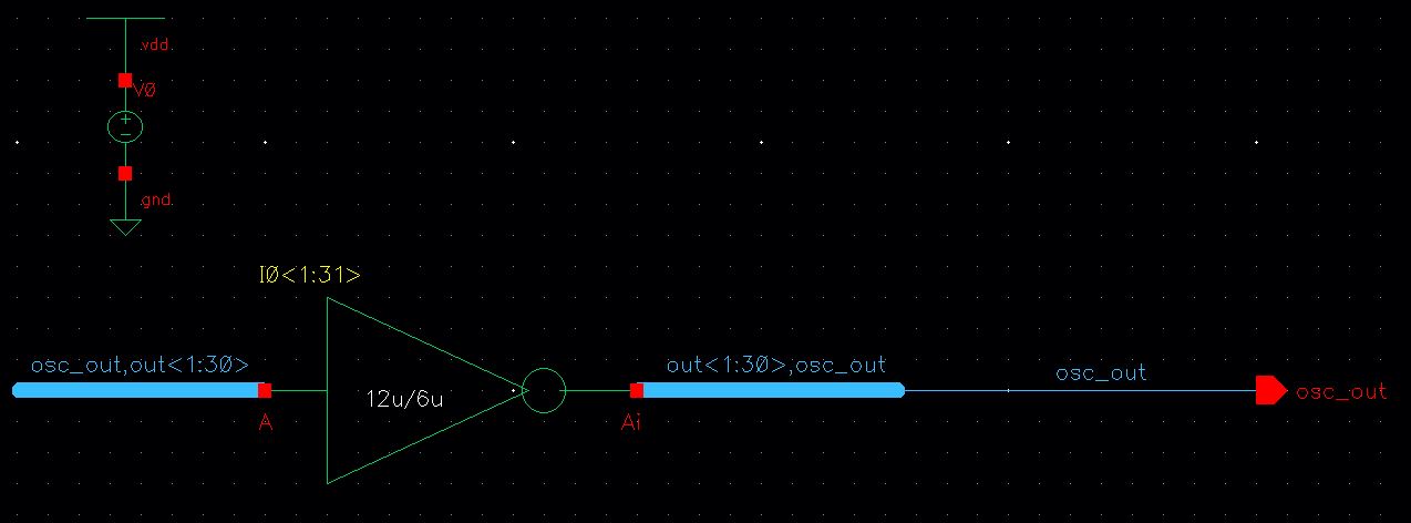
I created the
layout by instantiating 31-inverters and connecting them in series as shown. I
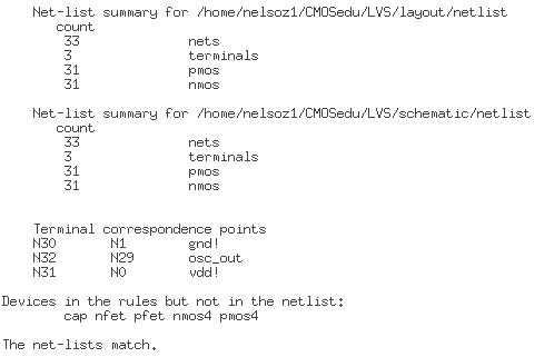
then made sure the layout passed DRC, and extracted it and continued to make
sure that the Layout matched the Schematic.


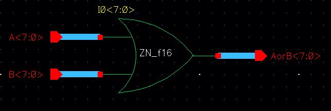
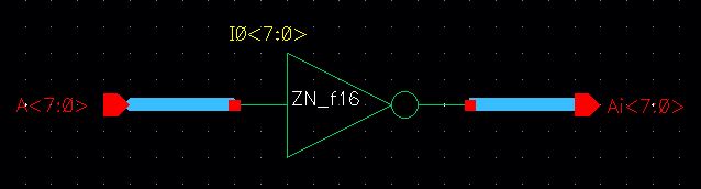
Experiment 2: 4-bit Inverter/Bus and
Array experiment
I then went on
to create a 4-bit inverter that was required to gain practice with bus and
array design.
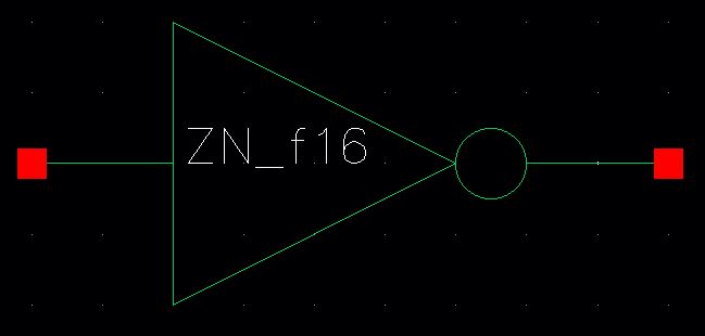
I first made
the inverter and made a symbol for it.
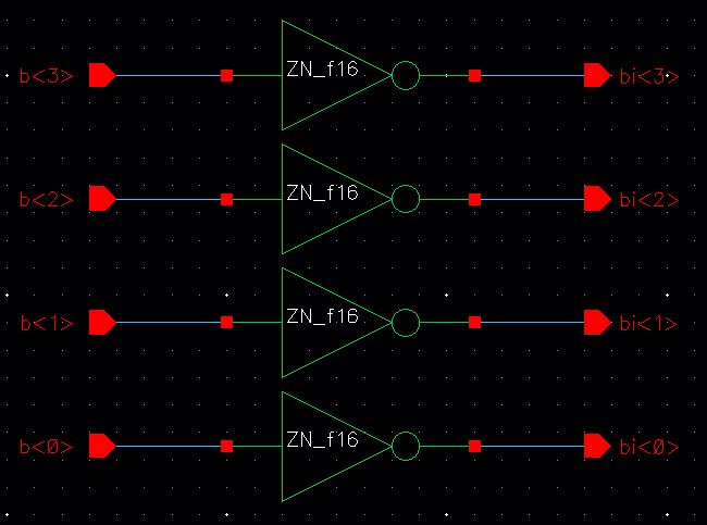
Then I used
that inverter and instantiated it 4 times and created 4 pins representing 1 bit
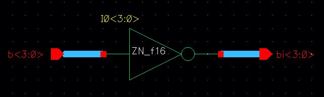
of an array (0 to 3, <3:0>). Using the idea from that schematic I created
another schematic where I used a 4-bit array in a bus
connecting it to a 4-times instantiated inverter and connected a 4-bit array in
a bus in the output. I then created a symbol of that schematic and simulated
its operation.
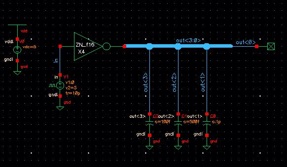

You can see
that the effect of the capacitive load on the inverter will have a major
influence on the delay in the rise and fall time. The larger the capacitive
load, the longer the delay. You can see the difference in the delay from the 100f
F capacitor and the 1p F capacitor is substantial.
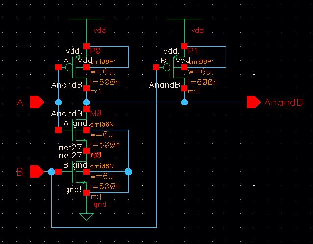
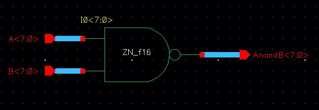
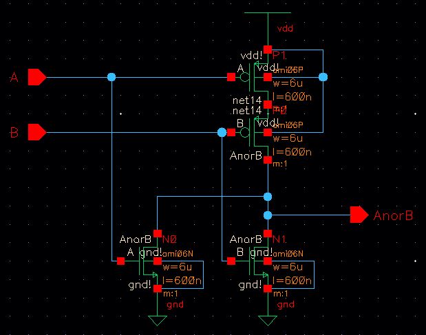
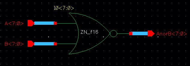
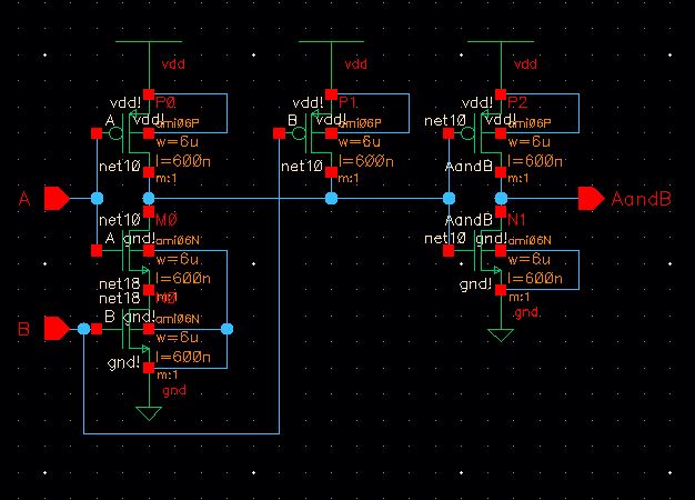
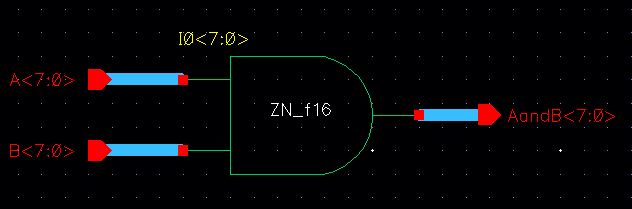
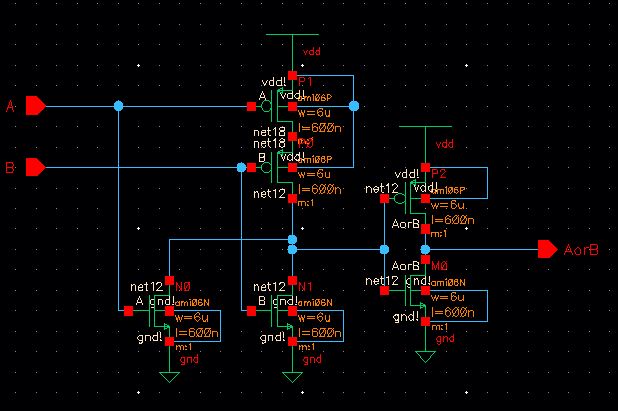
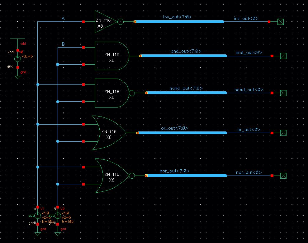
Experiment 3: 8-bit Inverter, NAND,
NOR, AND, OR
I then went on
to create 8-bit gates that were required to gain practice with bus and array
design.
I would design
the schematic and then create a symbol for it. Using that symbol I would
connect a bus to the inputs and outputs and rename the instance to give it an
8-bit width.
 |
 |
 |
 |
 |
 |
 |
 |
|
 |
I then went on
to test the 8-bit gates.

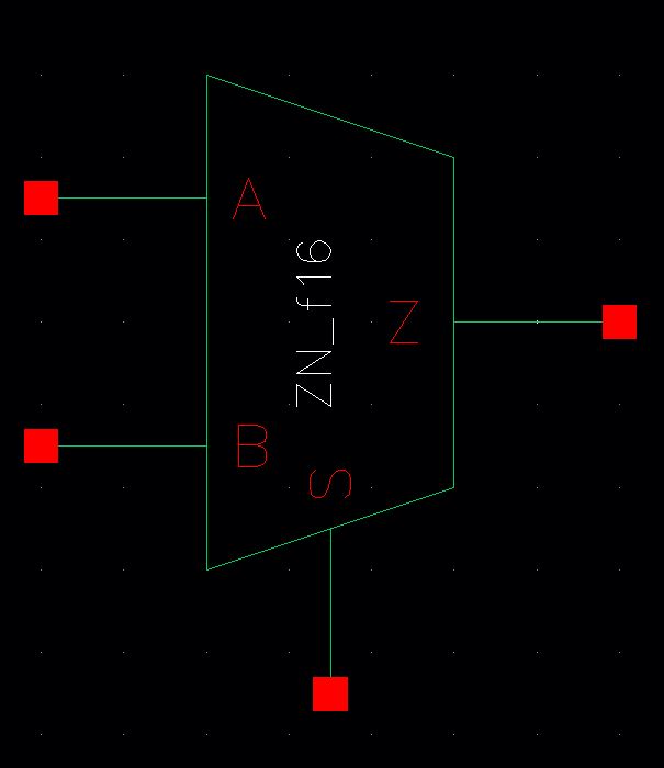
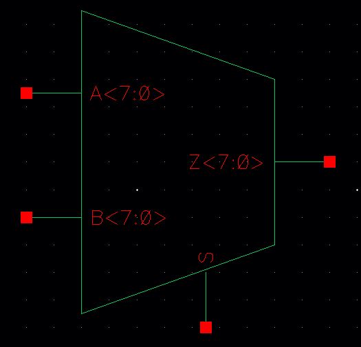
Experiment 4: 8-bit MUX/DEMUX
I created the
schematic of the MUX/DEMUXer using an inverter on the
selector input to allow for one selector input as opposed to two, and then
created a symbol for it.
The reason it
is a MUX and DEMUX is because you can use it either as a selector to decide
WHAT gets fed through, or as selector to decide WHERE it gets fed through to. I
then went to build my 8-bit MUX/DEMUX by instantiating it 8 times and
connecting 8-bit array busses to the inputs and outputs. I then went to
simulate as a MUX first to ensure proper operation.
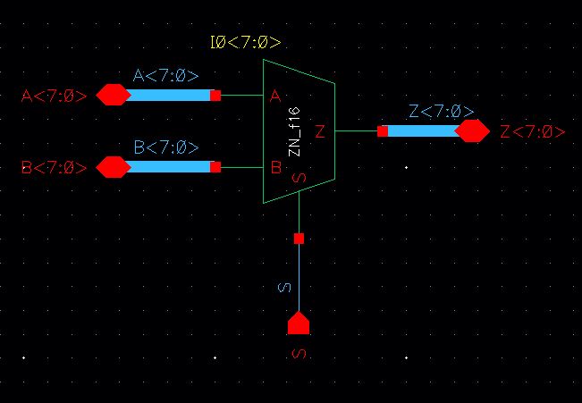
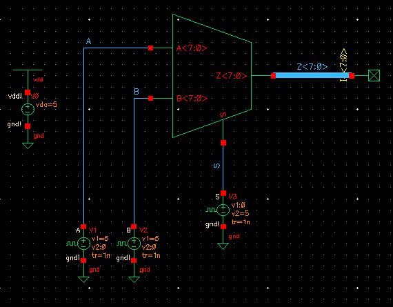

I then went on
to simulate it as a DEMUX.
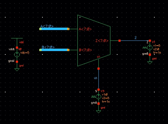

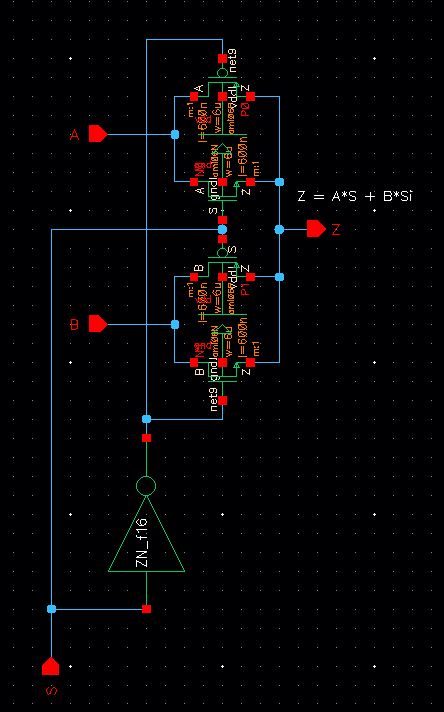
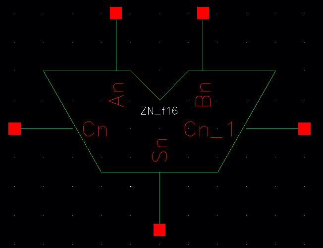
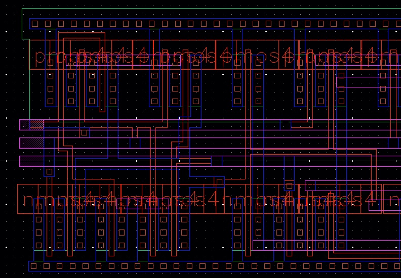
Experiment 5: Full Adder and 8-bit
Full Adder
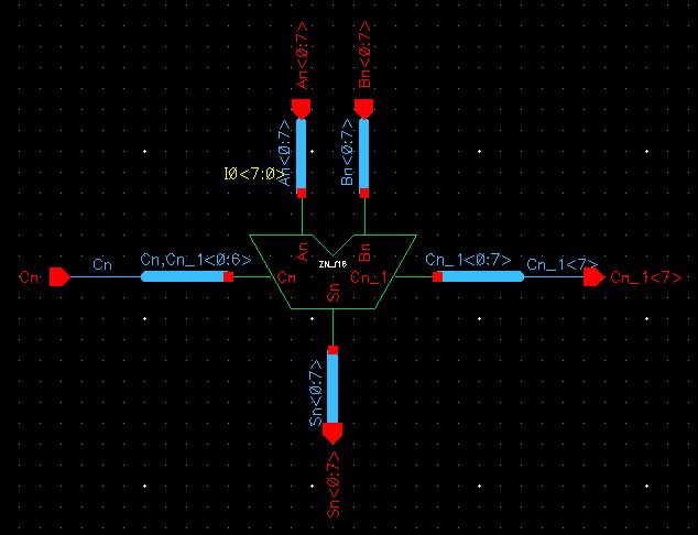
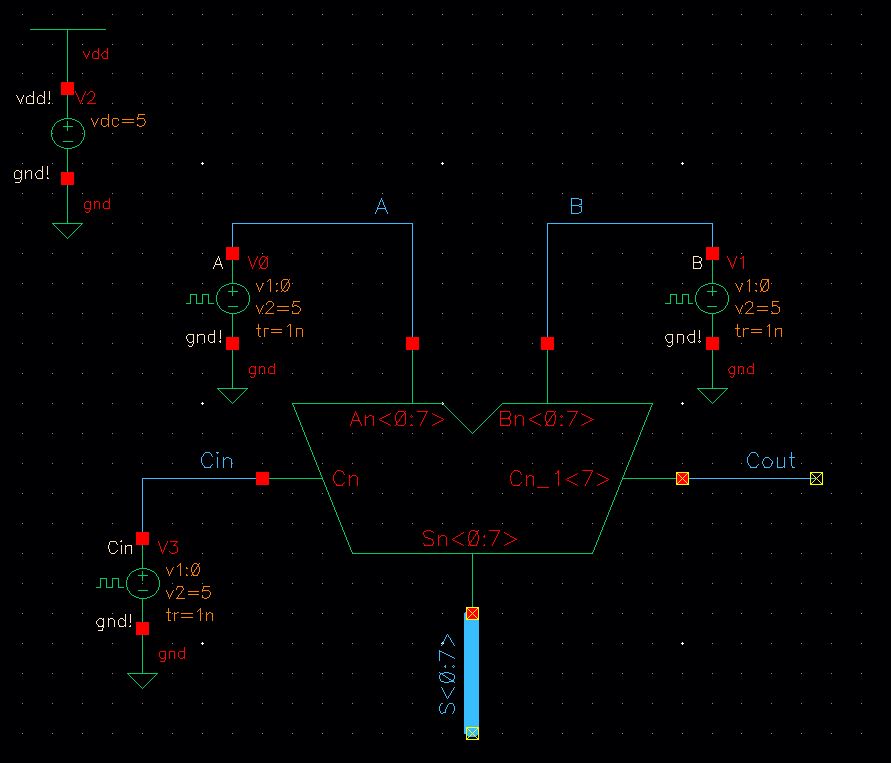
Next I went on
to make the full adder shown in Fig 12.20 of the textbook. I also used the
inverter that has been used previously in this lab to create this design. I
then went on to simulate the design operated as expected.

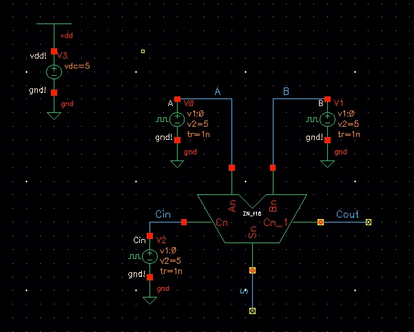

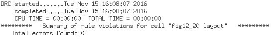
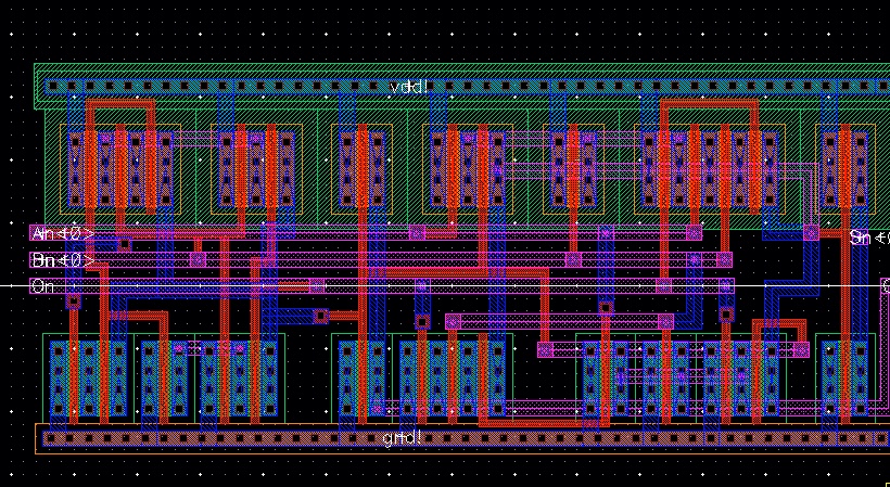
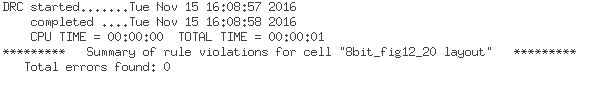
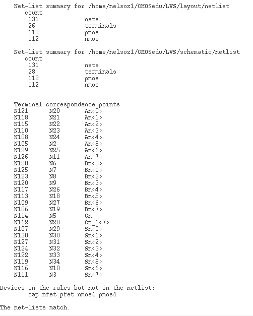
After
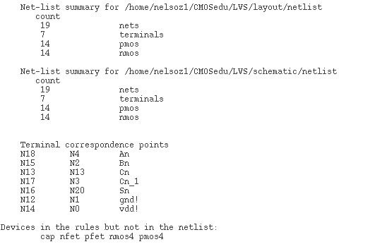
simulating I went to layout, extract, DRC, and LVS the design.


From here I
was able to create an 8-bit Full Adder in a similar fashion to how it has been
done previously in this lab and simulated it.

From here I
went to instantiate my Full Adder layout and then route and place the pins. I
then extracted, DRC’d and LVS’d
my design.


I’ve attached my lab7 repository below