Lab 6 - EE 421L
nelsoz1@unlv.nevada.edu
Pre-lab:
Finish Tutorial_4 ✓
Back-up
all previous work from Lab and the course work ✓
_________________________________________________________________________________________________________________________________
Lab
Experiment 1:
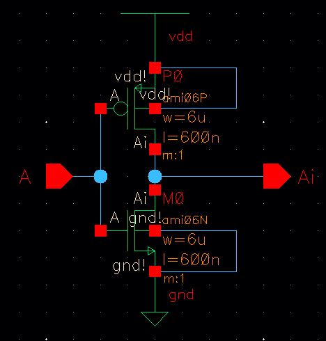
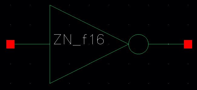
The
first task was to go through Tutorial_4, which involved using the inverter from
the previous tutorial. I used 6u/0.6u PMOS and NMOS for the inverter.
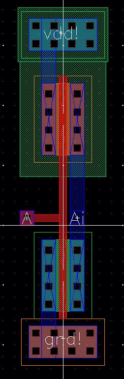
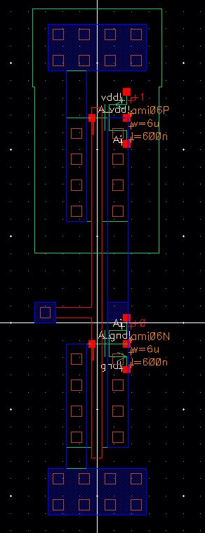
I’ve
laid out the inverter and shown the schematic, symbol, layout, and extracted
views.
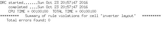
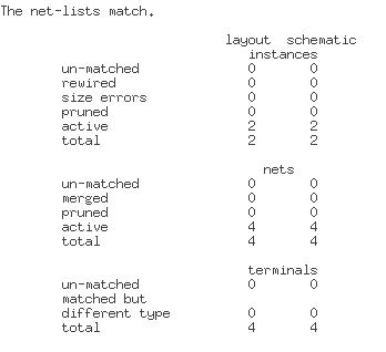
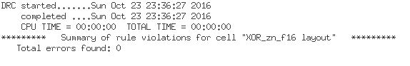
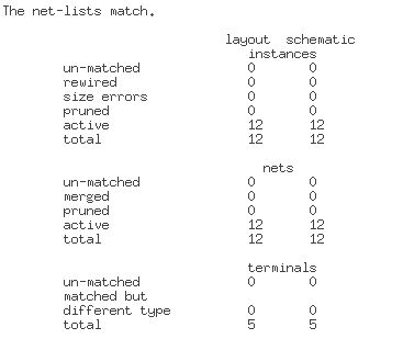
I also was
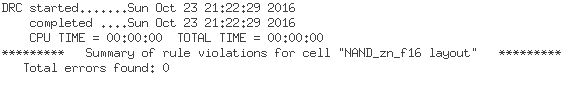
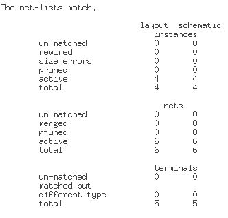
able to verify the inverter passed DRC and LVS
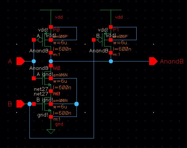
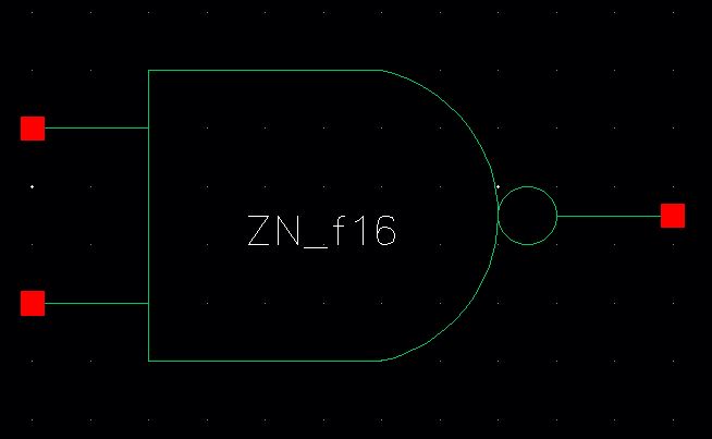
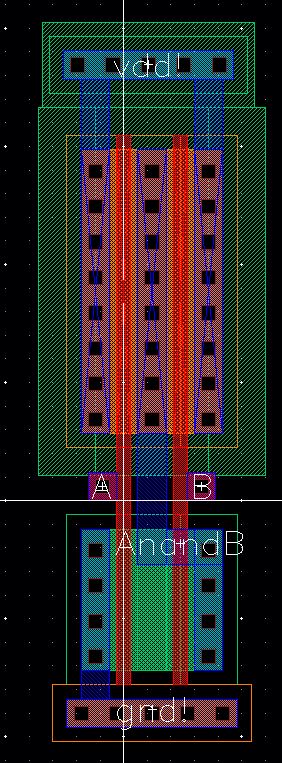
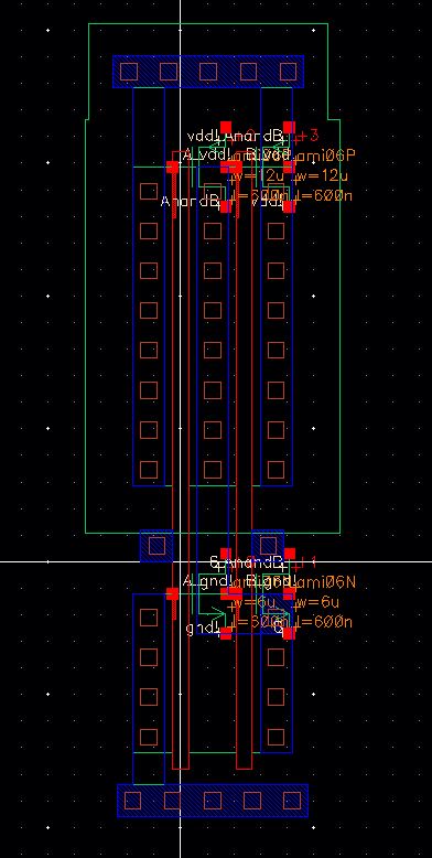
Next, I went
to build the NAND gate, also using the same parameters as the inverter, it is
6u/0.6u PMOS and NMOS
I’ve
laid out the NAND gate using the NMOS and PMOS and shown the schematic, symbol,
layout, and extracted views.
As shown in
Tutorial_4 we used the flattening property to remove contact cuts from the NMOS
Experiment 2:
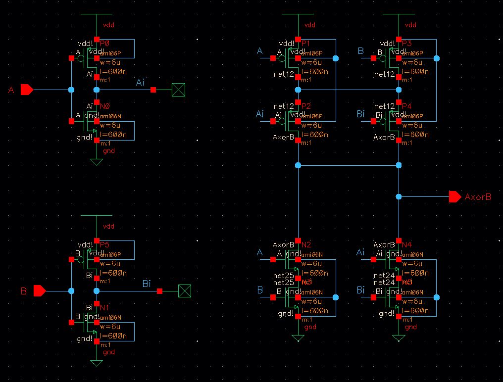
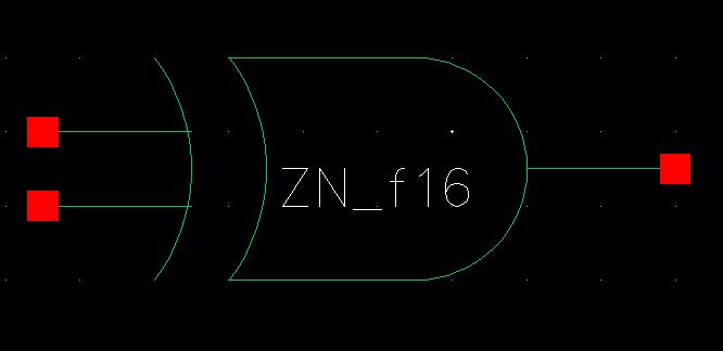
The second
portion of this lab involves making an XOR gate
We are able to
use the inverter to build the input interfaces of the XOR. From there A, Ai, B,
Bi are routed in the PMOS/NMOS configuration shown below.
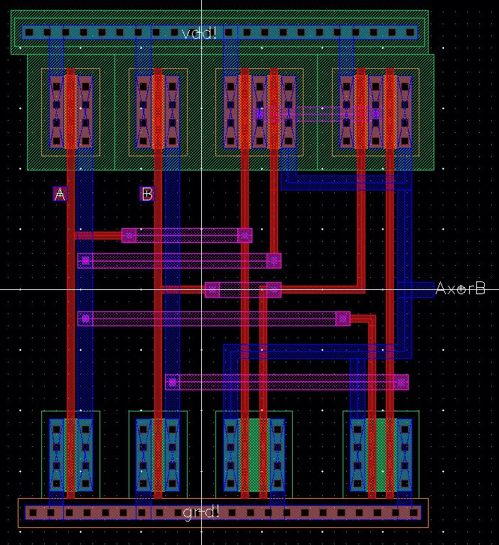
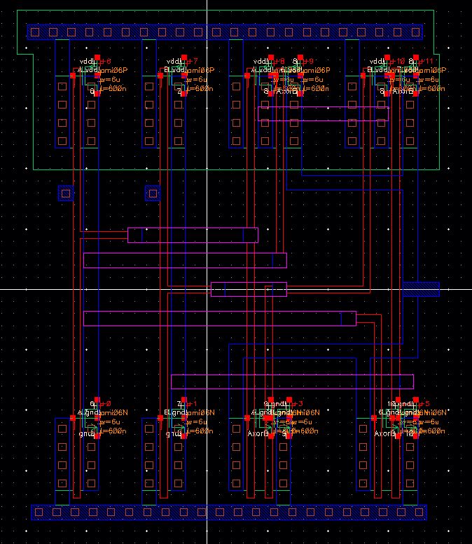
I laid out the
XOR and shown the schematic, symbol, layout, and extracted views.
I created an ntap and ptap strip at the top
and bottom of the layout to tie vdd! and gnd! to.
I used metal2,
m1_poly, and m2_m1 vias to make connections from the
different inverter, PMOS, and NMOS components used to create the layout. The
metal2 layer was used so that I wouldn’t be shorting any connections
while crossing across the metal1 layers.
I have all the
components necessary to create the Full Adder, but I want to simulate the
different gates I’ve created before moving onto the Full Adder design.
|
A |
B |
ANANDB |
|
0 |
0 |
1 |
|
0 |
1 |
1 |
|
1 |
0 |
1 |
|
1 |
1 |
0 |
|
A |
B |
AXORB |
|
0 |
0 |
0 |
|
0 |
1 |
1 |
|
1 |
0 |
1 |
|
1 |
1 |
0 |
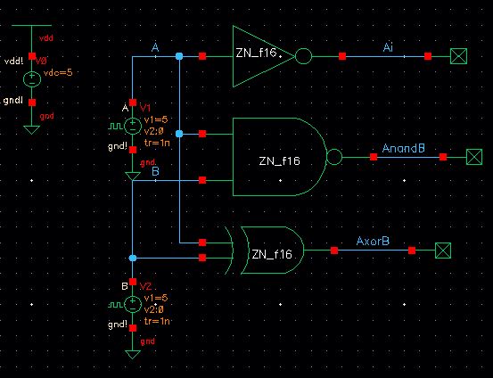

You can see
that the gates are operating as expected when compared to the truth tables. I
set the input pulses A and B on different periods, as well as different pulse
widths to get varied inputs.
Experiment 3:
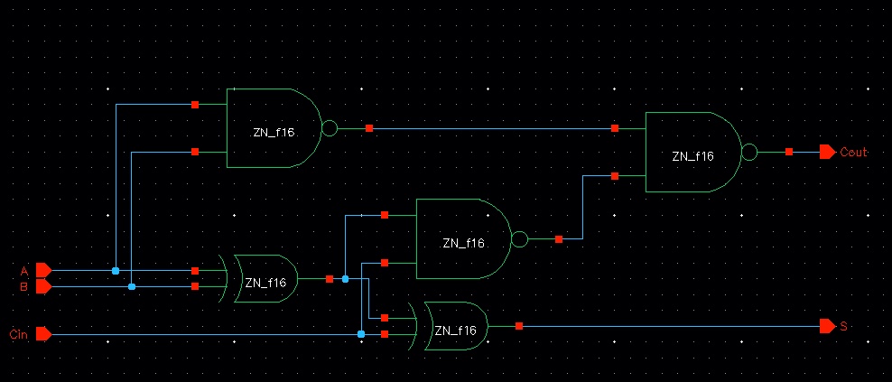
The last
experiment in the lab was to create the Full Adder. To create the Full Adder I used the previously created XOR and NAND gates. I
instantiated their symbols in the schematic to build the full adder which
required 3 NAND gates and 2 XOR gates. It accounts for inputs A and B, as well
as a Carry-In bit. It outputs the Sum as well as a Carry-Out bit. Using the
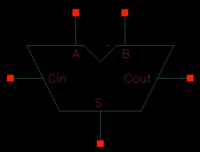
Full Adder schematic we created the standard symbol
used for adders in industry.
To layout the
Full Adder I copied the NAND and XOR gates into new cells so I could slightly
modify them to remove the gnd! and vdd! pins so that I could create one uniform power and
ground strip. I instantiated the modified NAND and XOR layouts and then used
the metal3 layer to make the connections, which necessitated the use of m3_m2 vias, as well.


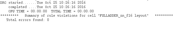
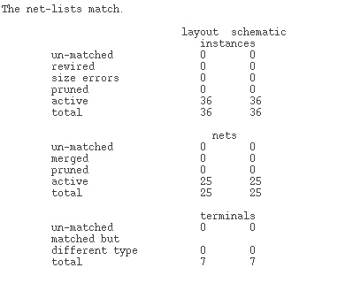
Now I want to
test the schematic and extracted layout to ensure that it is working properly.
|
A |
B |
Cin |
S |
Cout |
|
0 |
0 |
0 |
0 |
0 |
|
0 |
0 |
1 |
1 |
0 |
|
0 |
1 |
0 |
1 |
0 |
|
0 |
1 |
1 |
0 |
1 |
|
1 |
0 |
0 |
1 |
0 |
|
1 |
0 |
1 |
0 |
1 |
|
1 |
1 |
0 |
0 |
1 |
|
1 |
1 |
1 |
1 |
1 |
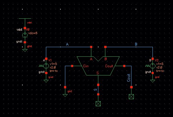

The
simulations show that our Full Adder produced the expected result.
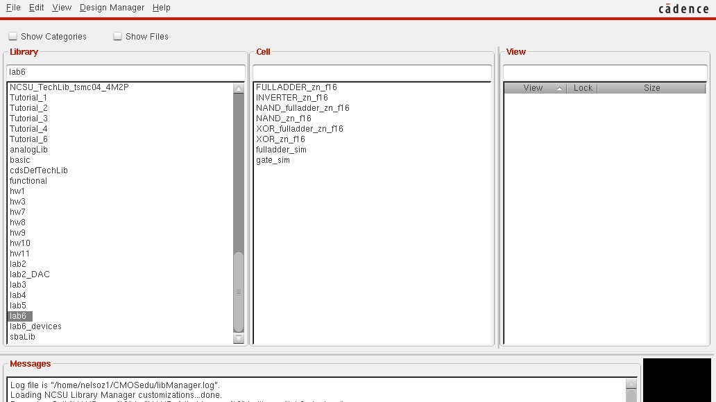
I've named all my cells using my initials and indicated the semester that I am taking the class
I’ve
attached my lab6 repository below