Lab 5 - EE 421L
nelsoz1@unlv.nevada.edu
Pre-lab:
Finish Tutorial_3 ✓
Back-up all
previous work from Lab and the course work ✓
_________________________________________________________________________________________________________________________________
Lab
Experiment 1:
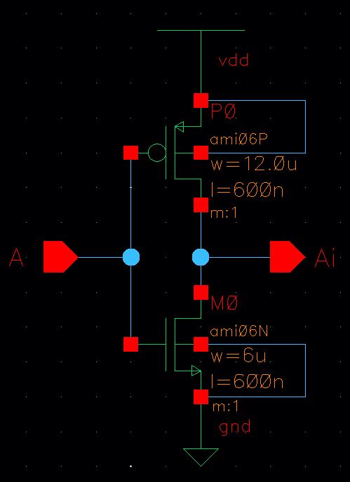
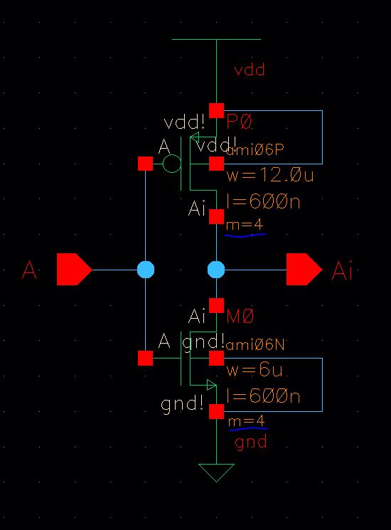
The first task
was creating a CMOS inverter using a 12u/0.6u PMOS and 6u/0.6u NMOS
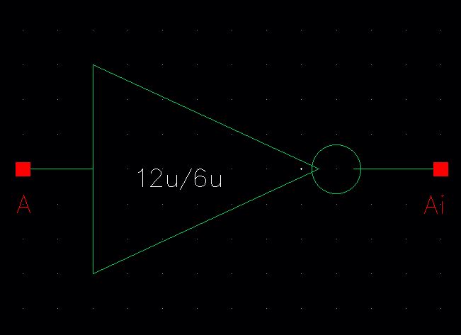
I built a
schematic for the inverter along with the indicated symbol from Tutorial_3. In
the schematic I used a VDD supply net as opposed to a DC Source.
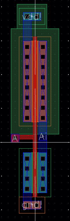
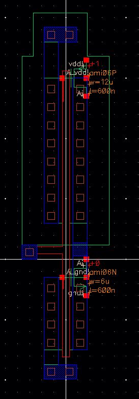
After I built
the schematic I began building the layout of the CMOS, verifying DRC after
major installments.
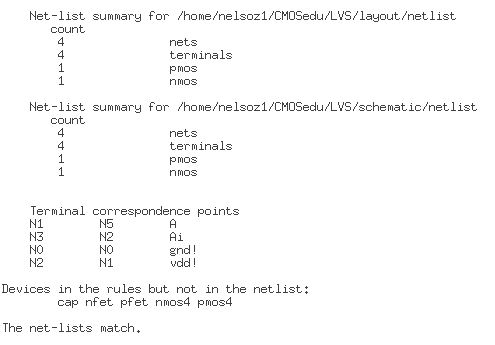
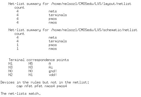
All pins in
the layout were named to match the pins in the schematic so that the LVS of the
Extracted layout would be a breeze, and the netlists did match.

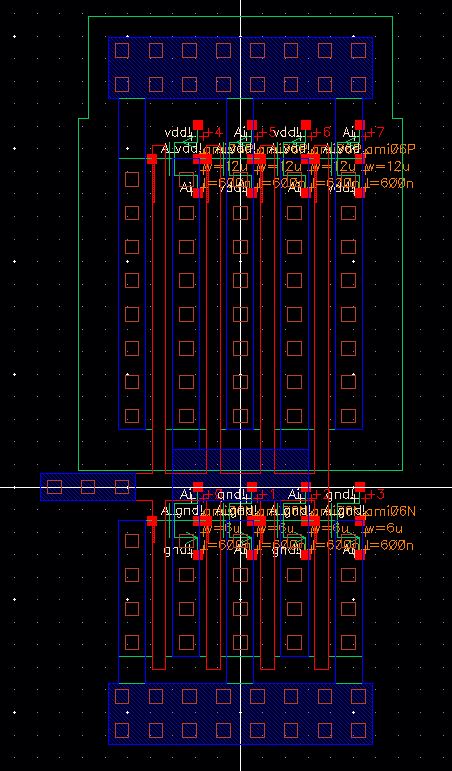
Experiment 2:
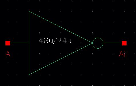
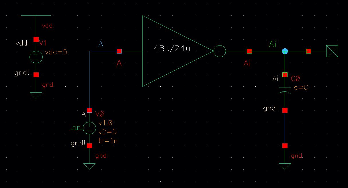
Next I began
to build PMOS/NMOS schematic with a 48u/24u that is 4x the size of the previous
experiment. I built the schematic and set the multiplier (m) on each MOS device
to 4 and created an additional symbol as well.
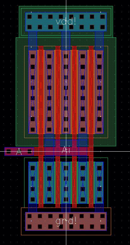
After building
the schematic I went to layout the CMOS like I did previously in Experiment 1,
and made sure to consistently DRC the layout and after extraction, went on to
LVS it and found that the netlists matched.

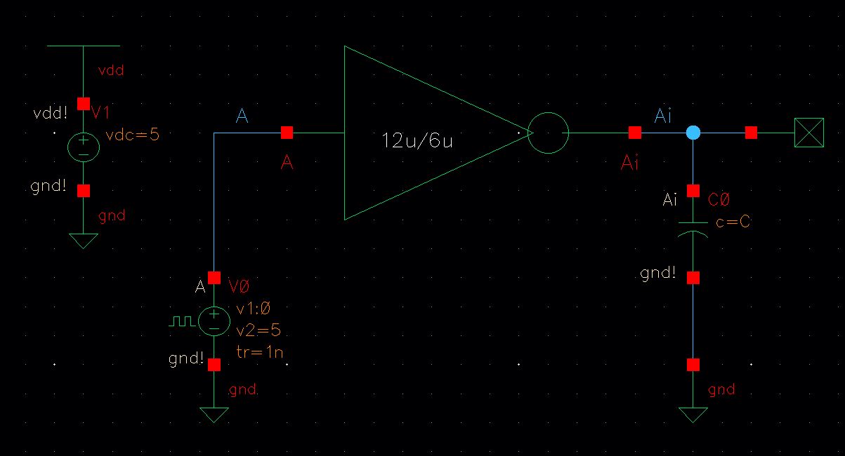
Experiment 3:
Now that I
have layouts and matching schematics I can move onto the simulations portion of
the lab. I will simulate these layouts/schematics using Cadence’s Spectre, and UltraSim. I am simulating the schematics in a transient sweep varying
the capacitance from 100f F to 100p F.
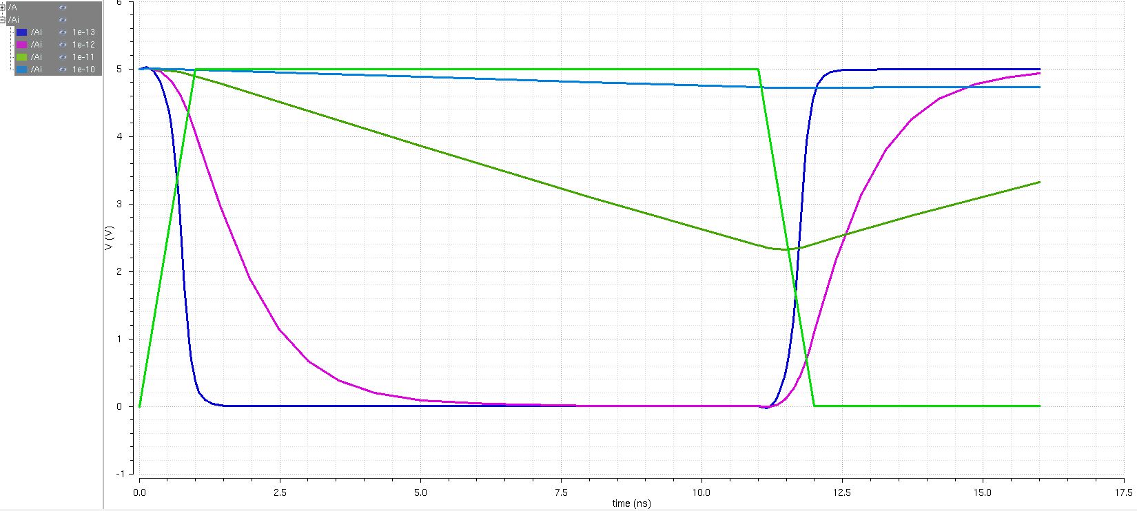
First I will
show simulations done using Spectre.
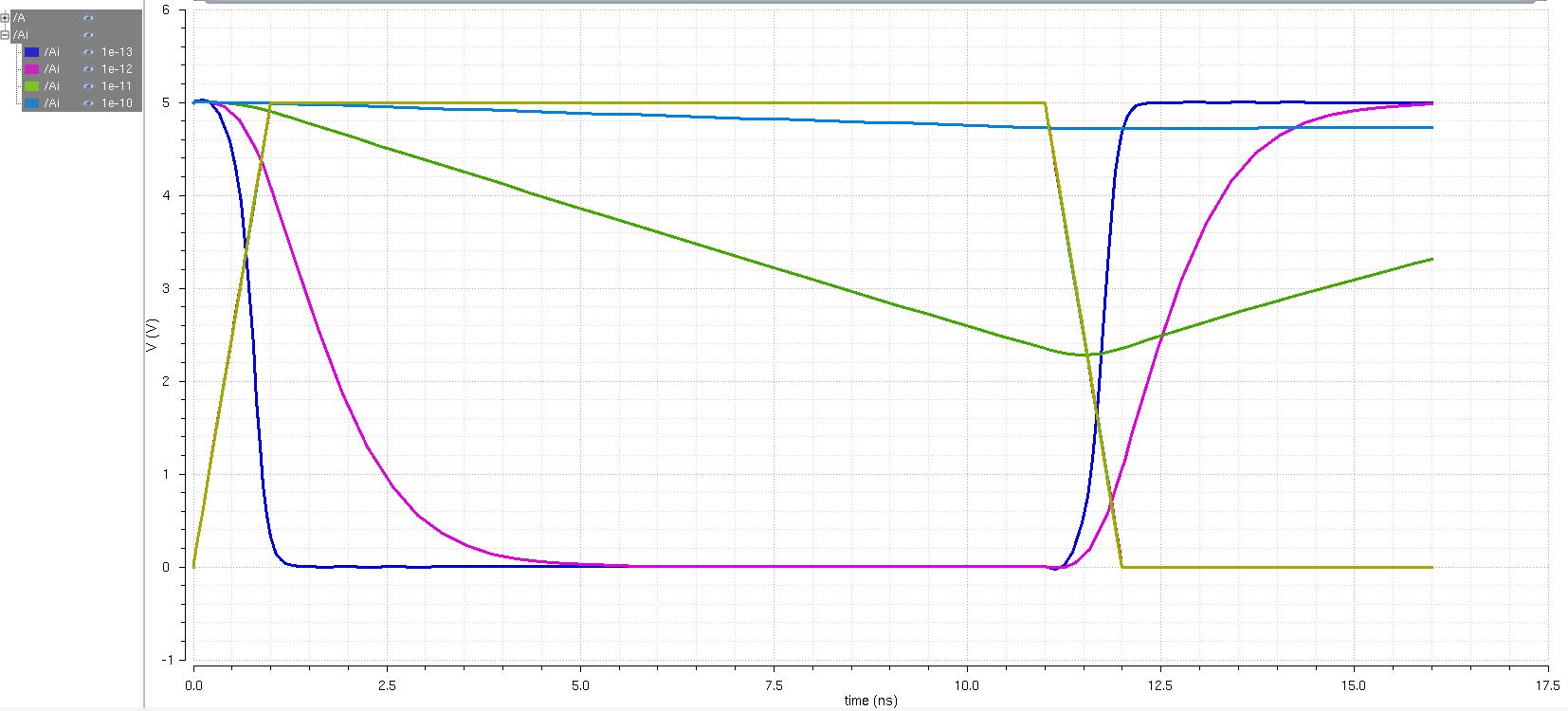
Given the graph, the 100f F capacitor is the blue line, the 1p F capacitor is the purple line, the 10p F capacitor is the green line, and the light blue line is 100p F line.
As the capacitance increases the inversion takes much longer
Also I have
the simulations done using UltraSim.
The
simulations of Spectre and UltraSim are nearly identical, but UltraSim has slightly clearer/resolute
simulations for viewing.
Experiment 4:
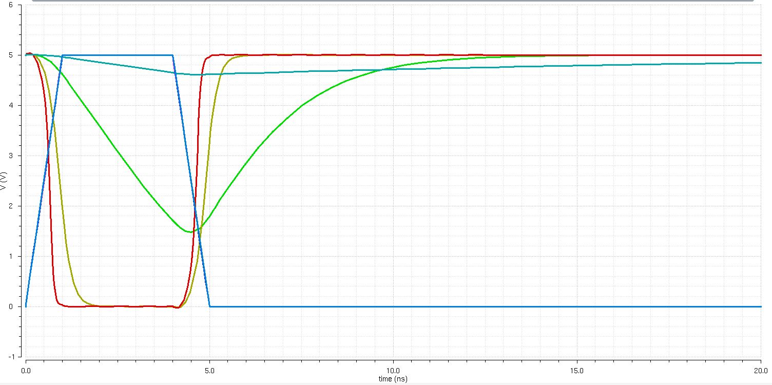
I will repeat
what I performed in Experiment 3 again but using the CMOS that is 48u/24u, and
for it I built another simulation schematic, and began sweeping the same
capacitive loads from 100f F to 100p F.
First I ran
simulations using Spectre.
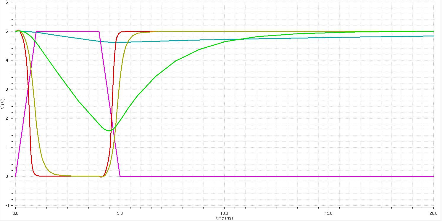
Also I have
the simulations using UltraSim.
__________________________________________________________________________________