Lab 4 - EE 421L
nelsoz1@unlv.nevada.edu
Pre-lab:
Finish Tutorial 2 ✓
Make sure the
body of all NMOS devices (p-substrate) are at ground and body of PMOS devices
(n-well) are at VDD ✓
Back-up all previous work from Lab 2 and the course work ✓
________________________________________________________________________________________
Lab
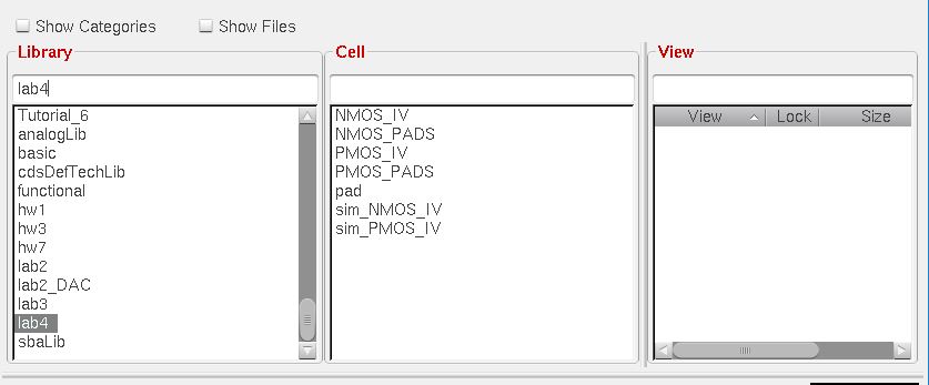
Library Manager for lab4
Experiment 1:
First I copied the files from Tutorial_2 into a new library titled
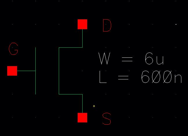
lab4 to use in this lab. Using the NMOS schematic I created a symbol to
represent it to test using the IV tracing curves. The body of NMOS4 was
connected to ground.
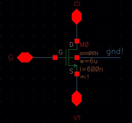
I made an NMOS
schematic and then went on to vary the voltages VGS or VDS
or both.
NMOS
dimensions were 6 um x 600 nm (W/L)
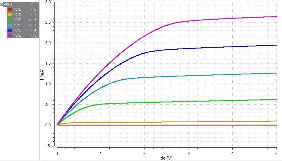
The first IV
curve traced was ID vs. VDS where VGS sweeps
from 0 to 5 V in 1V increments, and VDS sweeps from 0 to 5 V in 1mV
increments
The waveform
indicates a different VGS voltage going from the bottom to the top
(0 – 5 Volts)
I generated
the waveform by plotting the current at the drain (ID), and the
voltage of drain-source (VDS) and varying the gate-source (VGS)
voltage
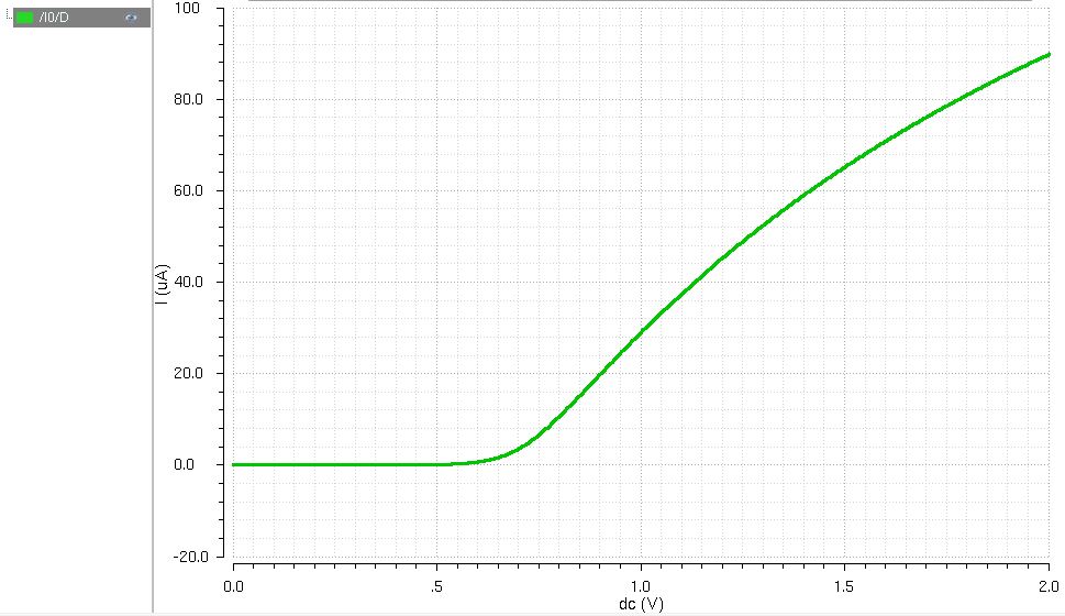
The second IV
curve traced was ID vs. VGS where VDS is fixed
at 100 mV and VGS sweeps from 0 to 2 V in 1 mV increments
The waveform
indicates the NMOS conducting current after the threshold voltage (VGS
> VTH) has been reached, the curve begins to increase.
I generated
the waveform by plotting current at the drain (ID) and the
gate-source (VGS) voltage
Experiment 2:
I repeated the
experiments for PMOS that we did with the NMOS
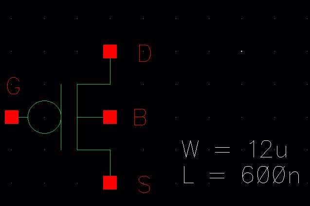
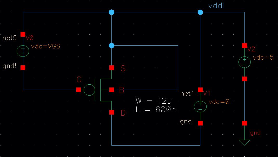
I made a PMOS
schematic and then went on to vary the voltages VGS or VDS
or both.
PMOS
dimensions were 12 um x 600 nm (W/L)
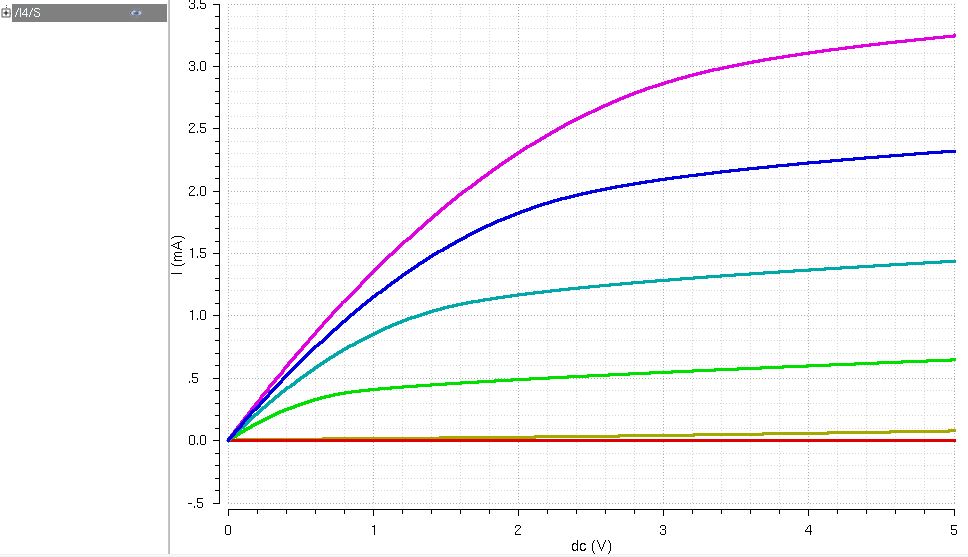
The first IV
curve traced was ID vs. VSD where VSG sweeps
from 0 to 5V in 1V increments, and VSD sweeps from 0 to 5 V in 1mV
increments
A major
difference between the PMOS and NMOS structures was that we require a
connection between the source and VDD in order to have enough
potential for the PMOS to conduct. The waveform looks similar to that of the waveform
produced from the NMOS in the first experiment, contributing to the theory of
corresponding VSG values
I generated
the waveform by plotting the current at the drain (ID), and the
voltage of source-drain (VSD) and varying the source-gate (VSG)
voltage
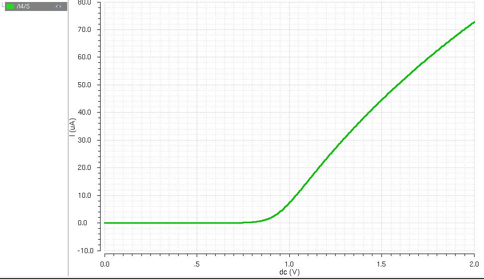
The second IV
curve traced was ID vs. VSG where VSD is fixed
at 100 mV and VSG sweeps from 0 to 2 V in 1 mV increments
I generated
the waveform by plotting current at the drain (ID) and the source-gate
(VSG) voltage
Yet again, as
VSG approaches the threshold voltage, the PMOS begins to conduct current, and
the curve increases.
Experiment 3:
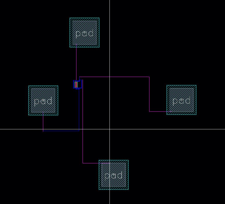
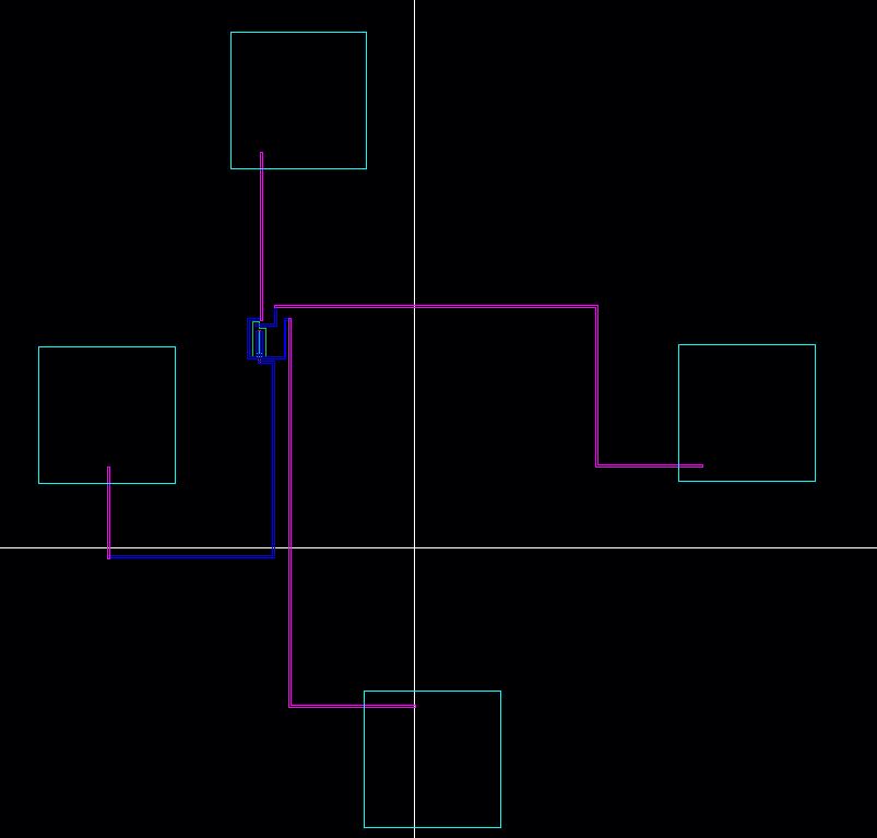
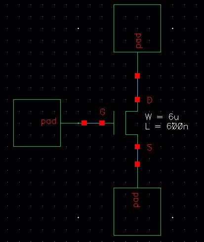
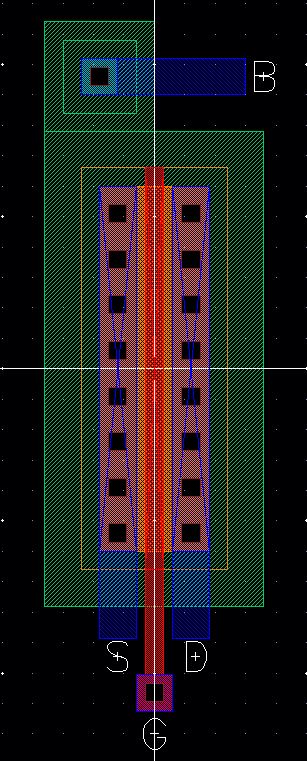
I went on to
build the NMOS layout with dimensions 6 um x 600 nm (W/L) that are connected to
probe pads
To make the
process easier I used the probe pads that I made while going through Tutorial_6
and copied the pad cell (which includes layout, schematic, and symbol) into my
lab4 library
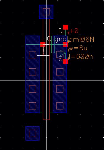
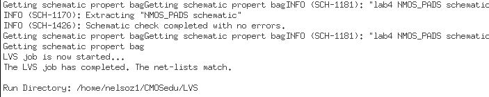
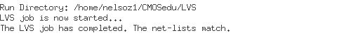
From here I went to layout the NMOS (like done in Tutorial_2) following the given specifications and the Layout and Extracted views are shown below. I then verified that it passes LVS and DRC.
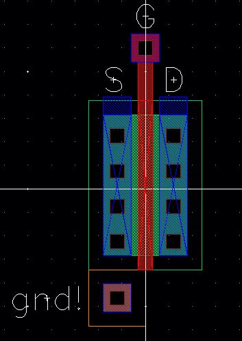

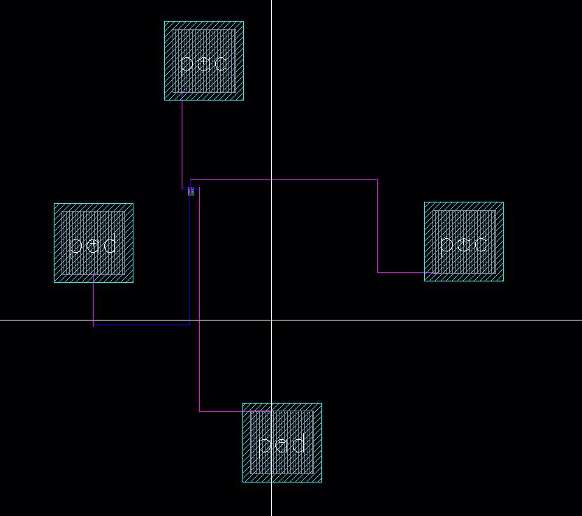
Then to
hook-up the probe pads to the NMOS I used the metal3, metal3_metal2, metal2,
metal2_metal1, and metal1 layers. I descended the layers of metal3 to metal1 as
I worked from the probe pads to the NMOS.
Experiment 4:
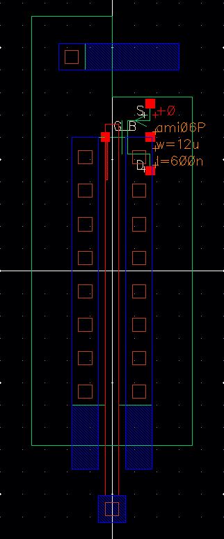
I went on to
build the PMOS layout with dimensions 12 um x 600 nm (W/L) that are connected
to probe pads
Yet again, to
make the process easier I used the probe pads that I made while going through
Tutorial_6 and copied the pad cell (which includes layout, schematic, and
symbol) into my lab4 library
From here I
went to layout the PMOS (like done in Tutorial_2) following the given
specifications and the Layout and Extracted views are shown below. I then
verified that it passes LVS and DRC.
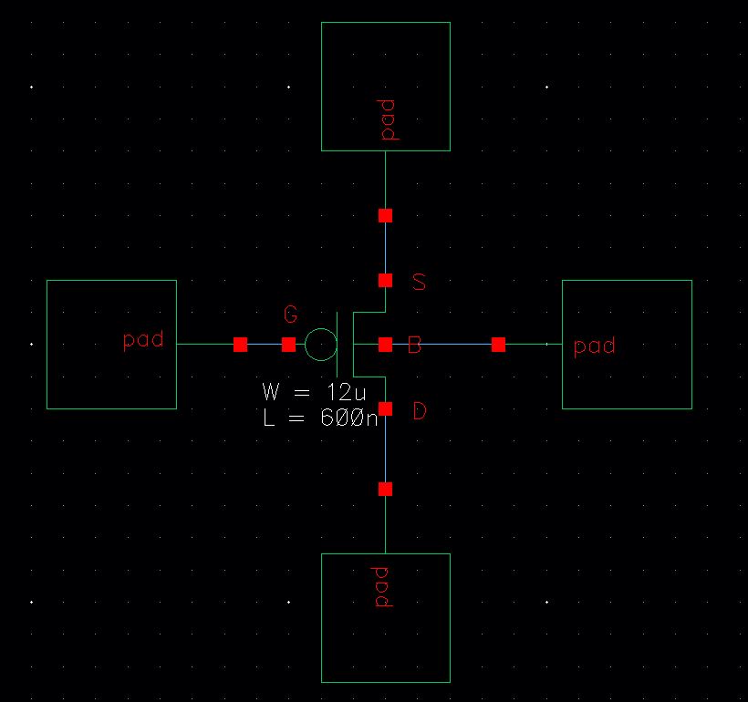

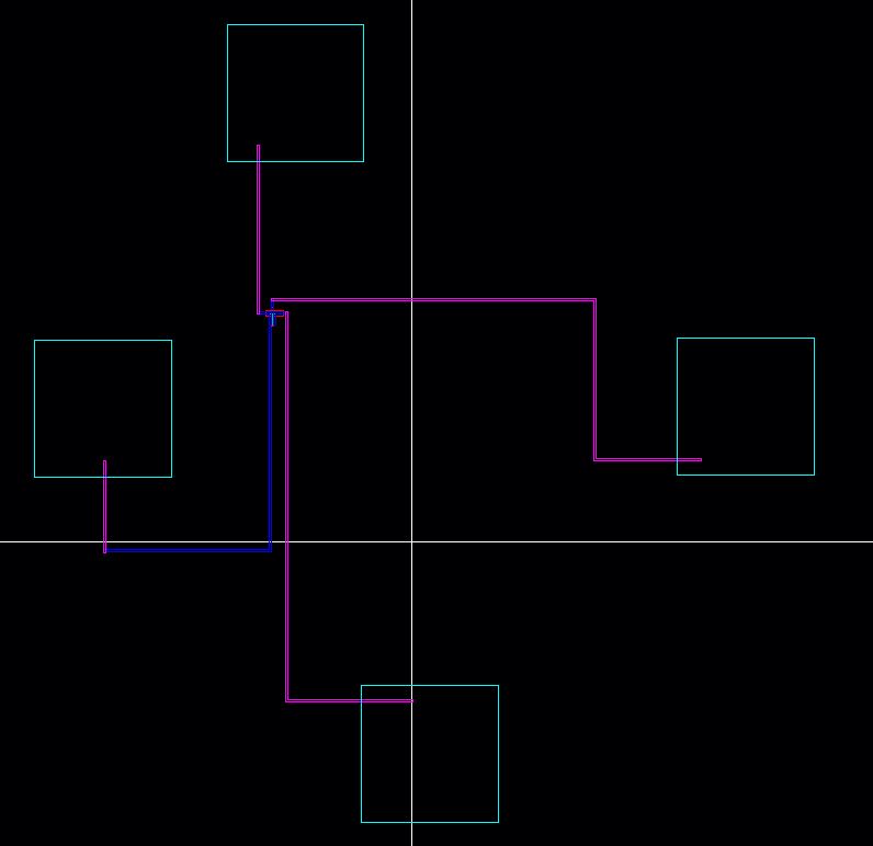
Then following
pretty much the same steps taken for the NMOS, I hook-up the probe pads to the
PMOS using the metal3, metal3_metal2, metal2, metal2_metal1, and metal1 layers.
I descended the layers of metal3 to metal1 as I worked from the probe pads to
the PMOS.