Lab 3 - EE 421L
LAYOUT OF A 10-BIT DAC (Digital-to-Analog Converter)
Pre-lab:
Finish Tutorial 1 (Creating a 10K N-Well Resistor) ✓
Back-up all previous work from Lab 2 and the course work ✓
________________________________________________________________________________________
Lab
Experiment 1: Creating the 10K N-WELL
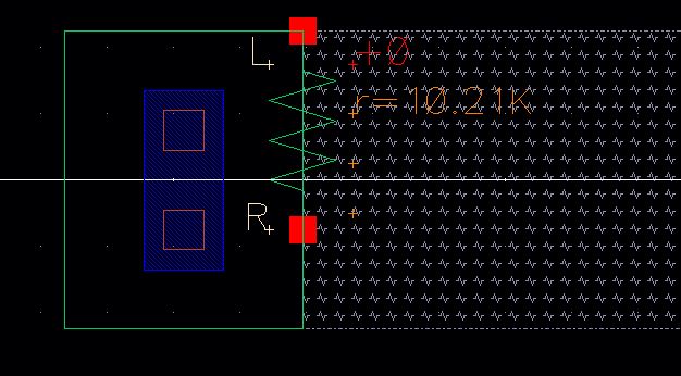
Using the information given by the process information from MOSIS, n-well material runs at about 800ohms/square, I solved the ratio that determines a Width-to-Height ratio that resulted in 12.5:1. Also necessary to keep in mind that the minimum width of an N-well is 3.6 microns (12 lambda where lambaa is 300 nm).The N-Well resistors Width is 56.1 microns and its Height is 4.5 microns. And the given width and height ratio is 12.47:1 which is right about where we want it to be.
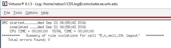
It DRC'd and when extracted came out to approximately 10k (10.21k)
Experiment 2: Creating DAC Layout
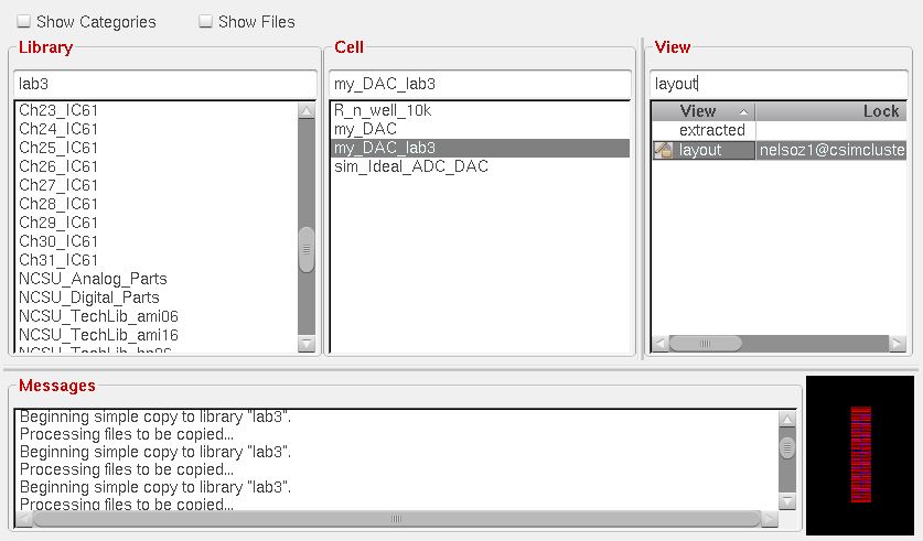
For Lab 3 I created a new library and copied the contents of my Tutorial 1 (10k N-Well Resistor) into it.
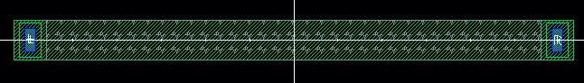
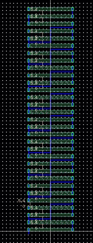
For the 2nd part of the lab I needed to start laying out the DAC (which is similar to the one created in Lab 2). To create the DAC I'm using the N-Well 10K resistor I just created. So I started from B0 and began working my way up the resistive ladder.
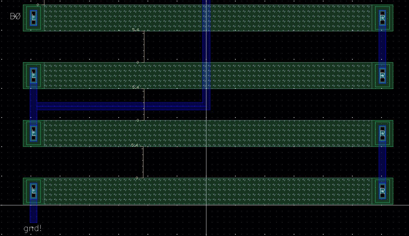
I used the shortcut key K to create rulers to expedite the design process, as there needs to be 5.4 microns of space between each N-Well resistor to pass DRC
From here I used the C key to copy and select the 3 top N-Wells for placement up the layout. I laid the N-Wells in parallel to create the ladder design that you see below. Doing that allowed me to create the 2R-R design that is necessary for the DAC
to be functional.
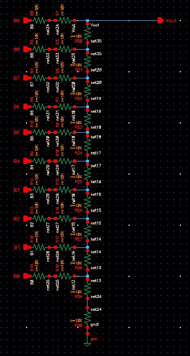
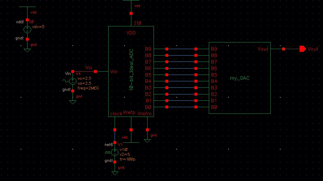
We use the DAC Schematic we created in Lab 2 as a comparison for the one we created in this lab.
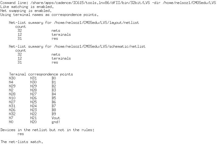
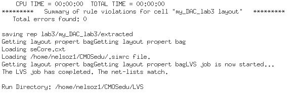
We verify that the Layout-Versus-Schematic (LVS) runs and that the netlists match their Schematic counterpart.
We also verify the DRC to make sure that it passes the pre-definied Rule-Checking process.
Then I replaced the symbol in sim_Ideal_ADC_DAC that i copied in to my lab3 library with a symbol created by my schematic
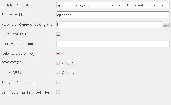
Now I prepared a simulation environment that will allow us to simulate our Layout as opposed to the Schematic we were previously simulating. I added "extracted" before schematic in the line labeled "Switch View List" to tell the simulator to simulate an extracted layout before it would begin to read from a schematic.
Experiment 3: Simulations
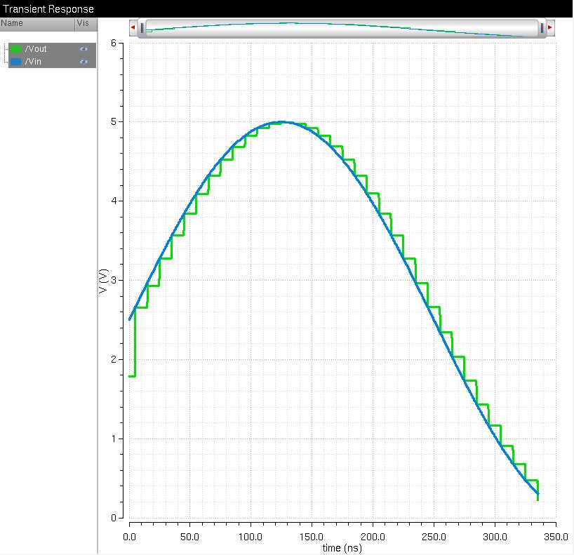
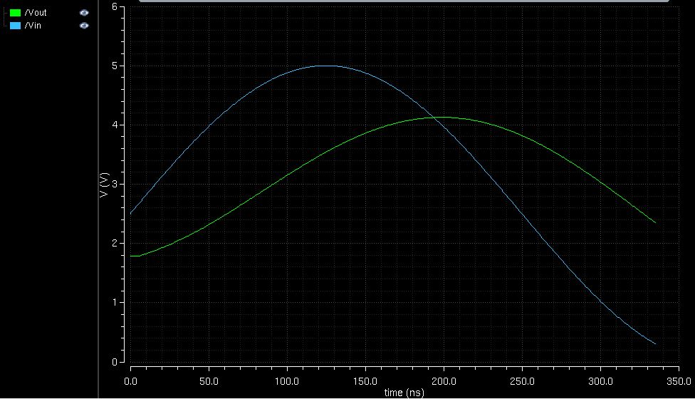
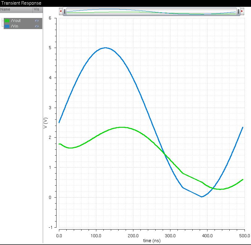
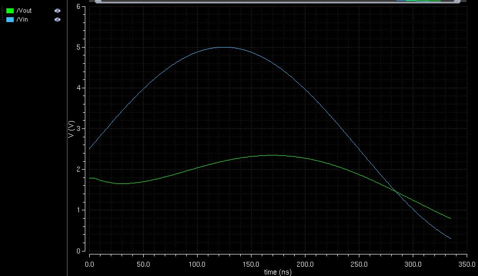
I performed the same simulations from lab2 as a comparison
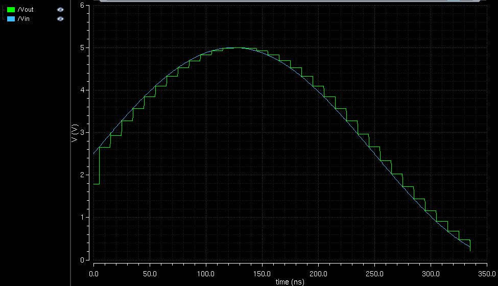
-Simulation 1 is the transient simulation with no load
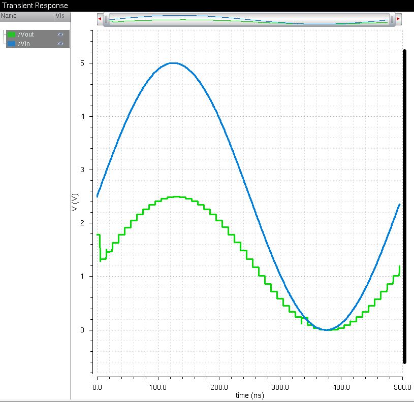
-Simulation 2 is the transient simulation with 10k resistor load
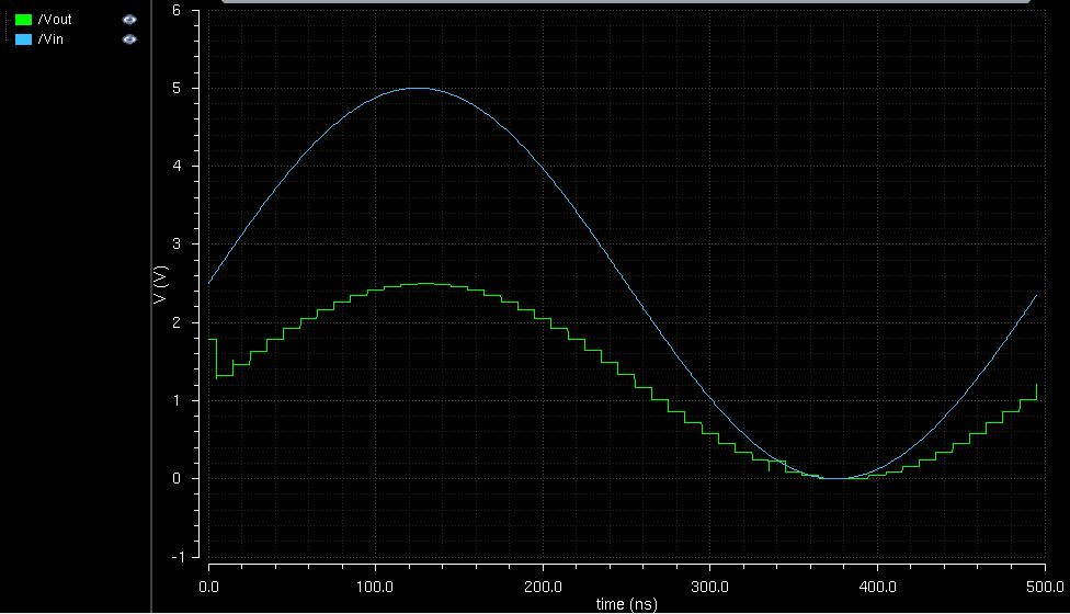
-Simulation 3 is the transient simulation with 10pF load
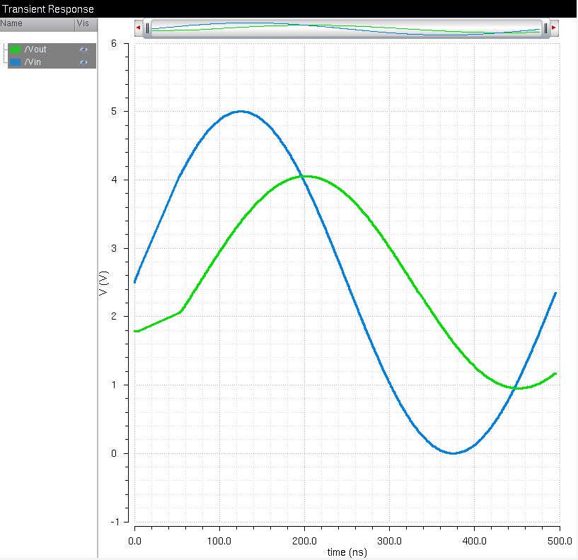
-Simulation 4 is the transient simulation with 10K and 10pF load
| Schematic Simulations | Extracted Layout Simulations |
 |  |
 |  |
 |  |
 |  |
I've provided below the link to the ZIP file containing all the work for Lab 3:
I've also included the definition for cdslib to make it easier:
DEFINE lab3 $HOME/CMOSedu/lab3