Lab 2 - EE 421L
DESIGNING A 10-BIT DAC (Digital-to-Analog Converter)
Pre-lab:
I downloaded the zipfile for lab2 to begin running the simulations. In cdslib I defined the library for lab2 and using MobaXterm I launched Cadence and in the library manager I had lab2 available.
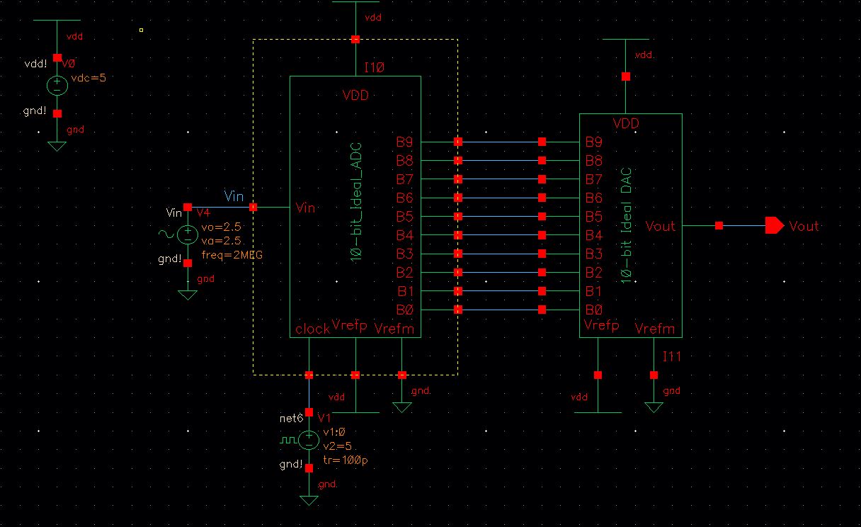
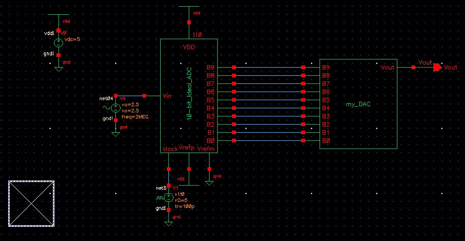
I opened up the schematic in the "sim_ideal_ADC_DAC" cell to view the following schematic.
Alongside the schematic I opened up the simulation state that was provided. I ran the simulation and then adjusted the background to be easier on the eyes as well as the trace properties to be a solid line and different colors.
Now, the ADC works by taking an input signal such as a sine wave and then outputing that sine wave translated into bits (in our case a 10 bit output design). The DAC reverses the work that the ADC does by rebuilding that signal using the bits.
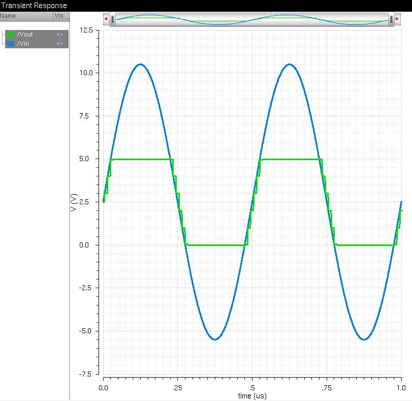
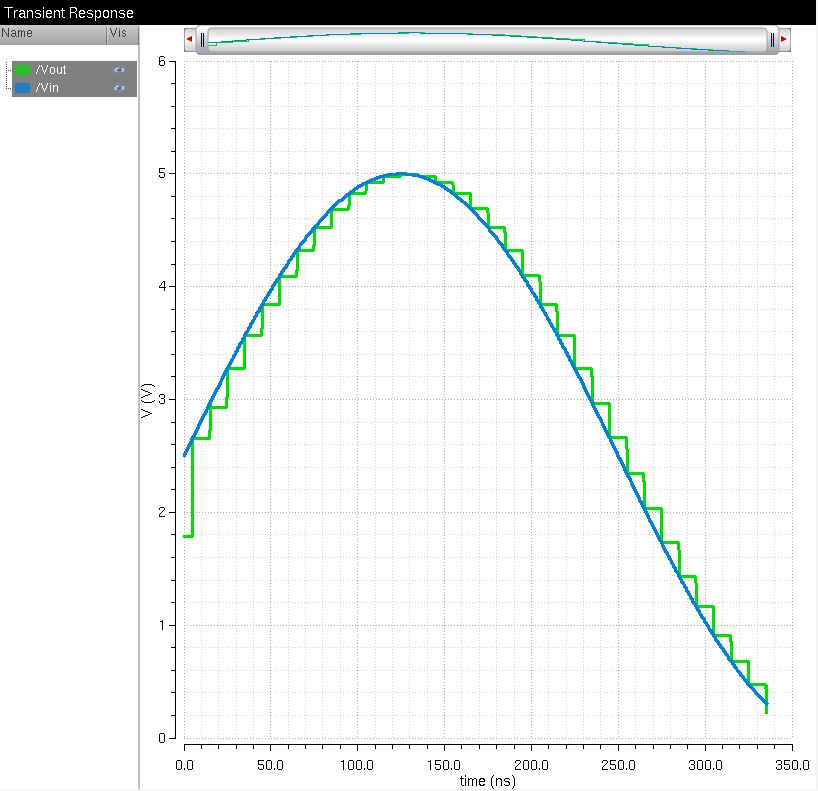
The ideal DAC is limited by Vdd as you cannot rebuild a signal with less power than the signal is supposed to carry. As shown in the image below when we treat Vin as an 8V sine wave you can see that the reconstructed analog signal is clipped at 5V level.
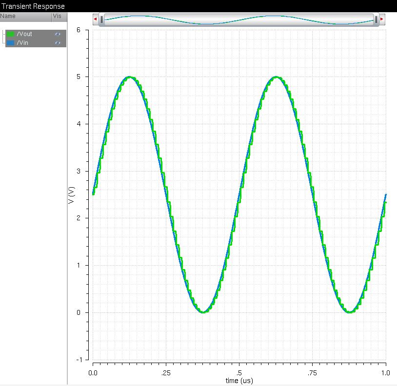
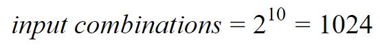
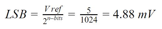
Since we have 10 bits, we have 1024 possible bit combinations which are built as steps from 0 V to 5 V.
Using this information you can determine that the LSB has a value of 4.88 mV, which basically means that it would require at least 4.88 mV to acheive a step or a bit.
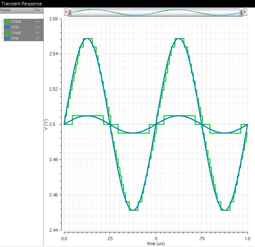
The image below shows a 4.88 mV signal which acheives 1 step from the signal, and a signal 10x that (48.8 mV) which gives 10 bitwise steps.
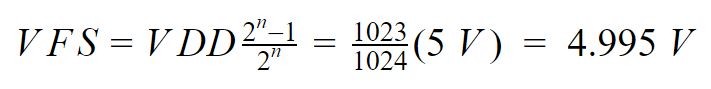
You can also determine the maximum voltage that can be reproduced from the 10 bit DAC, which is 4.995 V.
________________________________________________________________________________________
Lab
Experiment 1:
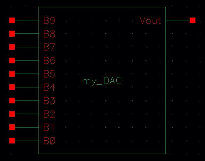
The first part of the lab involved designing our own DAC using 10K resistors. I setup a new cellview in lab2 titled "my_DAC". In that cellview I created a schematic and built the resitor divider using the 2R-R design.
I named all pins starting from B9 and going down to B0, as well as a Vout pin. The schematic shown below is the full design to be replacing the ideal DAC in the original "sim_ideal_ADC_DAC" schematic.
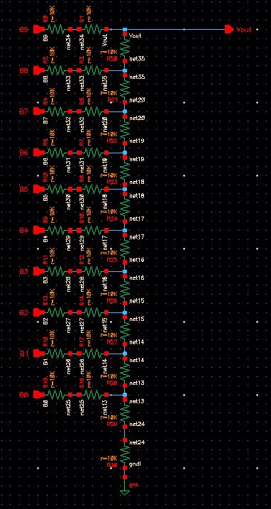
(Notice that the final resistive divider has 2R, which is necessary for the B0 pin)
Using DAC schematic above I created a symbol. Instead of copying (as recomended) I chose to create my own and then modify the original schematic even though it would be a little more work. I was able to create the symbol by Create -> Cellview -> From Cellview. The symbol is shown below.
Experiment 2:
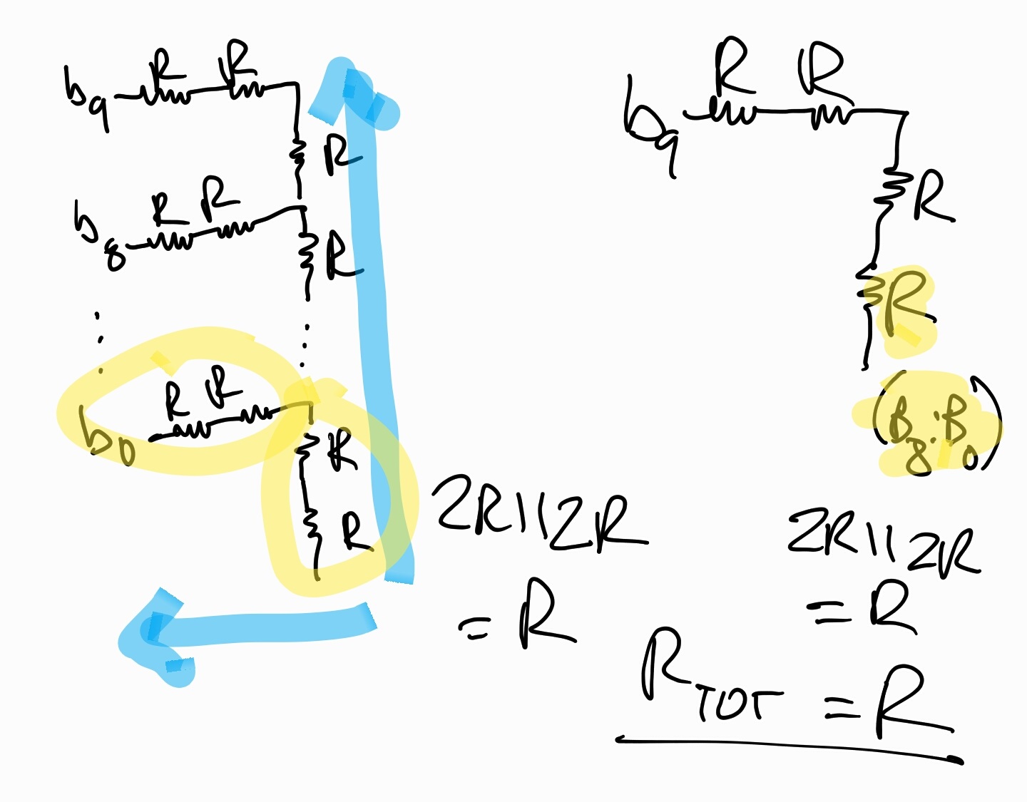
I was able to determine the output resistance of my_DAC by grounding all of the input pins (B9 : B0), and combining the resistors in series & parallel. After cascading up the resistive ladder if you will, you can see that the overall output resistance reduces to 10 kilohms.
Experiment 3:
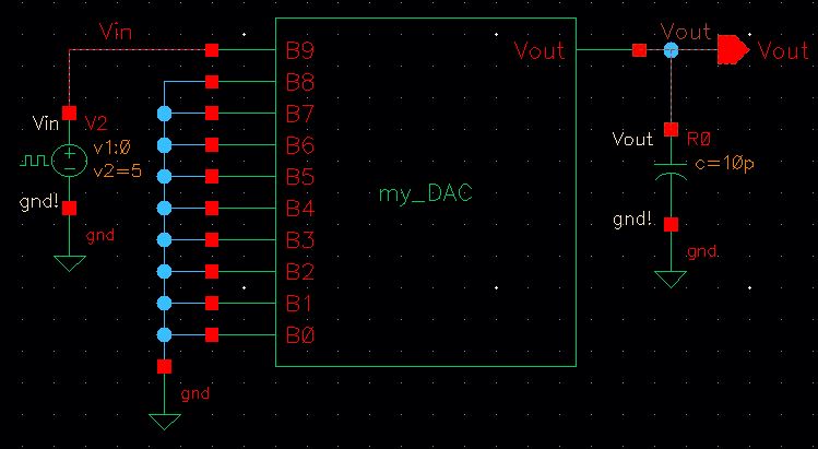
Now we want to show what kind of delay my_DAC experiences. To demonstrate that I built a circuit where my_DAC is connected to a pulse source that goes from 0 to 5 V with a 10 pF load. My schematic is shown below.
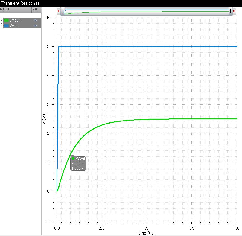
I calculated the time delay by:

I then used the schematic to launch ADE L, and created a test as well as set the traceable plots, being Vin and Vout. In the simulation below you can see that at 1.25 V (our expected halfway point, since Vout should be 2.5 V) that the time delay is approximately 70 ns.
Experiment 4:
It is now time to simulate a non-ideal ADC to DAC schematic. I copied the schematic from "sim_ideal_ADC_DAC" into my current cell, and then removed the Ideal DAC symbol and replaced it with my own, and then rearranged the pins to match my symbol. The schematic is shown below.
Using this schematic I was able to run the following simulations:
 | This is a simulation of my_DAC (non-ideal) with no load . You can see the difference between the ideal and non-ideal simulations because there are some minor differences and changes in signal (such as step accuracy) however it is pretty close to what we would hope for from a DAC. |
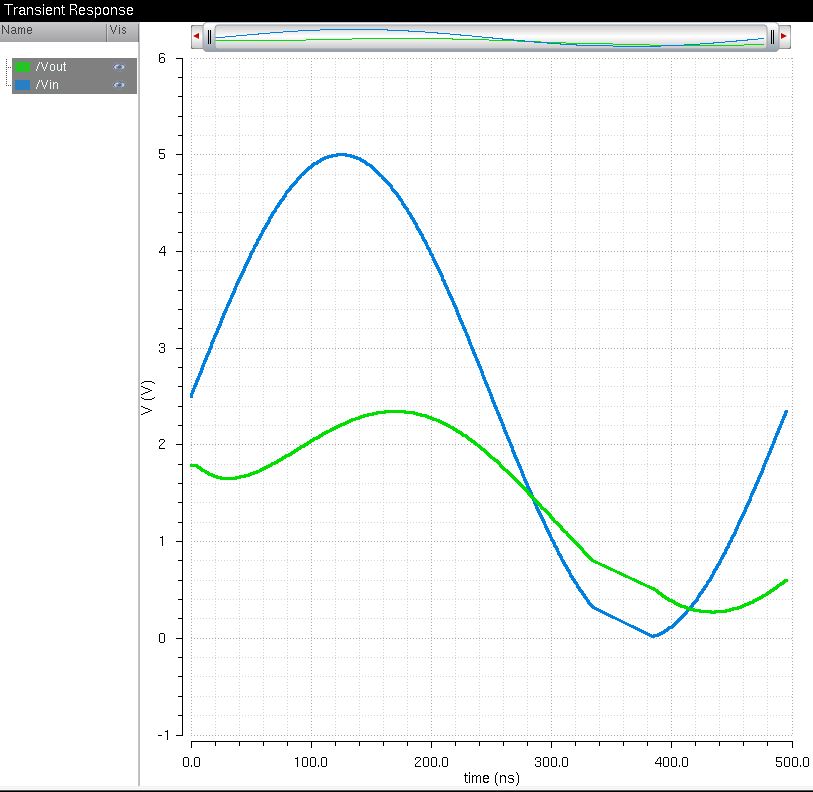
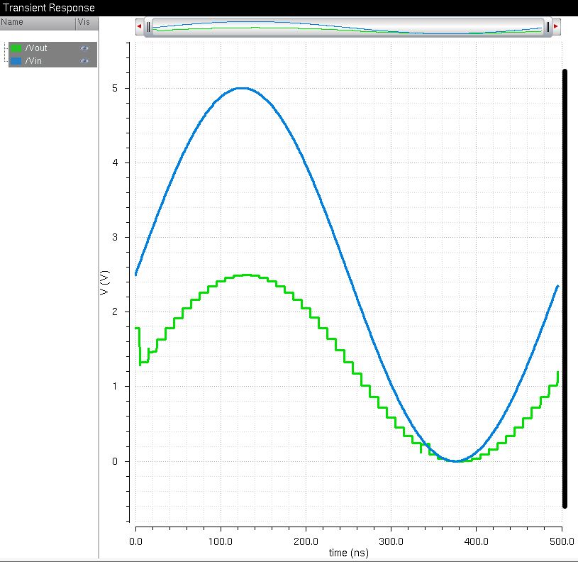 | This is a simulation of my_DAC (non-ideal) with a 10k load . You can see some of the major differences between the non-ideal with no load and non-ideal with 10k load simulations. The output voltage is greatly reduced due to the 10K load. This is, however, the expected result when driving a 10k load. |
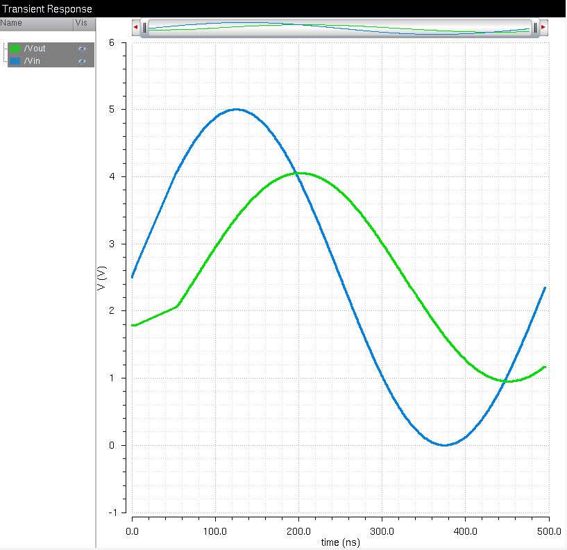 | This is a simulation of my_DAC (non-ideal) with a 10 pF load . You can see some of the major differences between the non-ideal with no load and non-ideal with 10 pF load simulations. The output voltage signal is much smoother and closer to the original input analog signal. It smooths the steps from the DAC however does implement a time delay by a factor very close to the one given in the schematic designed to test the time delay (approx. 70 ns). |
 | This is a simulation of my_DAC (non-ideal) with a 10 pF and 10K load . As you might expect, this simulation looks like a combination of the second simulation and the third simulation. The output voltage signal is much smoother (due to the factor of the capacitor) and reduced (due to the factor of the resistor ) compared to the original input analog signal. It smooths the steps from the DAC and drops voltage from the 10K load. As you can see, there is also an element of a time delay which is evident in the 3rd simulation. |
Discussion: Problems using transistors with a resistance that is high compared to R?
The issue with using switches (MOSFET) that have resistances that aren't << R are that you will inherit a loading effect which might diminish your output voltage, therefore it is much better to use aRm << R when implementing our DAC.