Project: Chip Layout
EE-421L
CHIP 3
Authored by
Ja Manipon
Carlos Lemus
Zach Nelson
maniponj@unlv.nevada.edu
lemus@unlv.nevada.edu
nelsoz1@unlv.nevad.edu
12/7/16
Lab Files
-
- First half of the project (just the detector
schematics, no layout), of your design and an html report detailing
operation (including simulations), is due at the beginning of lab on Nov. 16.
-
-
- Your detector circuit should show various inputs to verify it works
-
-
- Put your report (proj.htm) in a folder called /proj in your directory at CMOSedu.
-
- The second half of the project shows layouts, DRC, and LVS and extracted simulations
PART I

Info for testing
- Each test circuit requires its own power, but ground should be shared between the circuits on pad.
| Test Component | Power Supply Pin<i> |
| 2 input NAND gate | 18
|
| 2 input NOR gate | 23
|
| Inverter | 14
|
| 32-State Rign Oscillator | 11
|
2. When
testing with function generator use at least a 50 ohm resistor load.
For more information on why read this :
http://www.keysight.com/main/editorial.jspx?ckey=1948055&id=1948055&nid=-11143.0.00&lc=eng&cc=MY
3. Anywhere a power pin is required, apply a fixed 5V
4. NAND, NOR, and
Inverter gates have similar inputs to conserve space, check the output
pin to test each one seperately
5. Use probes to read data
2 Input NAND gate
Information
The 2 input
NAND gate takes in two inputs A and B and applies (AB)' to output
NAND_out. The NAND uses 6/.06 MOSFETS.
Schematic
|

|
Layout
|

|
How to Test
| Pin
|
Pin<i>
|
| A |
16 |
| B |
17 |
| NAND_out |
19 |
| Power |
18
|
Apply square wave function generator to A and B inputs.
| A |
B |
Out |
| 0 |
0 |
1 |
| 0 |
1 |
1 |
| 1 |
0 |
1 |
| 1 |
1 |
0 |
2 Input NOR gate
Information
The 2 input
NOR gate takes in two inputs A and B and applies (A+B)' to output
NOR_out. The NOR uses 6/.06 MOSFETS.
Schematic
|

|
Layout
|

|
How to Test
| Pin
|
Pin<i>
|
| A |
21 |
| B |
22 |
| NOR_out |
24
|
| Power |
23
|
Apply square wave function generator to A and B inputs.
| A |
B |
Out |
| 0 |
0 |
1 |
| 0 |
1 |
0 |
| 1 |
0 |
0 |
| 1 |
1 |
0 |
Inverter
Information
The inverter gate takes in one input A and applies A' to output Ai. The inverter uses 6/.06 NMOS and 6
12/.06 PMOS.
Schematic
|

|
Layout
|

|
How to Test
| Pin
|
Pin<i>
|
| A |
13
|
| Ai |
15
|
| Power |
14
|
Apply square wave function generator to A and the output should be the inverse.
NMOS
Information
The NMOS is 6/.06.
Schematic
|

|
Layout
|

|
How to Test
| Pin
|
Pin<i>
|
| G |
8 |
| D |
7 |
| S |
10 |
| B |
9 |
- Connect Drain to a fixed 5V power supply
- Connect Gate to increase the Gate voltage until current flows from Drain to Source. NMOS turns on when V(gate) is greater than V(threshold).
- Connect Source to GND
- Connect Body to GND
PMOS
Information
The NMOS is 6/.06
Schematic
|

|
Layout
|

|
How to Test
| Pin
|
Pin<i>
|
| G |
5 |
| D |
7 |
| S |
4 |
| B |
6 |
- Connect Drain to GND
- Connect Gate to decrease the Gate voltage until current flows from Drain to Source. PMOS turns on when V gate is 5V -V(threshold).
- Connect Source to fixed 5V
- Connect Body to VDD
Voltage Divider
Information
Schematic
|

|
Layout
|

|
How to Test
| Pin
|
Pin<i>
|
| 25k |
1 |
| 10k |
3 |
| divider out |
2 |
-
- To measure the 25K ohms resistor probe pin(X) and pin(Y).
- To measure the 10k ohms resistor probe pin(Z) and pin(Y).
- To
measure the output voltage of the voltage divider applay a known
voltage to pin(X) and use a multimeter to probe pad (Y) to get a
voltage with a 25k/10k ratio . Do Vout = 286m * Vin.
32-Ring Oscillator with Buffer
Information
Schematic
|

|
Layout
|

|
How to Test
| Pin
|
Pin<i>
|
buffer_out
|
12
|
power
|
11
|
Detector
Information
The
detector takes in input from the user (or a function generator). As the
clock reaches a rising edge, a bit from the input is shifted into the D
flip flop to the right. IF the input was 101011 and the output from the D Flip Flops is 101011 then the output will be high.
Schematic
|

|
Layout
|

|
How to Test
| Pin
|
Pin
|
| Input |
25
|
| Clk |
26
|
| Detector |
36
|
| Power |
27
|
The
fucntionality can be simulated using a peicewise function. You can try
something simlar to the image shown below on your function generator. Note, the input must be input from LSB to MSB.

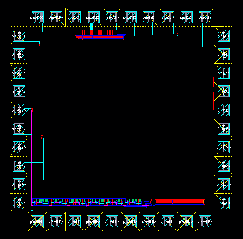
Final Layout
Return to EE 421 Labs